
  |
 |
|
Avaliable methods of research
- TOF SIMS
- Thermogravimetric and differential thermal analysis
- Impedance
- Testing of SOFC stacks
- Power electronics
- XPS
- Clean room for MEA production
- Bipolar plate production and tests
- SOFC tests
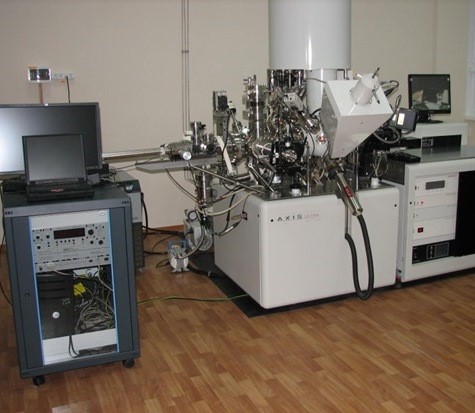
XPS
Ebinding=hn - (Ekinetic+j)
where hn corresponds to the X-ray photon energy, Ebinding is the kinetic energy of the electron emitted and j is the work function determined by the spectrometer characteristics and material properties. Therefore, the binding energy of the electron and the amount of the electrons with the given bonding energy (the position and intensity of the peaks on XPS spectrum) enables to identify the element, its chemical state and amount.
Auger electron spectroscopy (AES) is a modification of the photoelectron spectroscopy, where the adsorption of photoelectrons leads to a re-distribution of the electrons over the electron structure and emission of so-called Auger electrons from the top atomic layers. Since those eletrones are generally present on the sample surface, the method is applicable for surface investigations. AES allows to detect the presence of all the elements at the surface except for hydrogen and helium.
Electron spectrometer Kratos AXIS Ultra DLD is designed for investigation of the surface in ultra-high vacuum and allows to obtain the following information:
- Elemental qualitative and quantitative surface composition
- Chemical states of the elements at the surface
- Mapping of the element distribution over the surface
- Electron structure of the valence band
- Atomic structure of the surface of single crystals
Basic parameters:
- Sensitivity: 0.1 at. %
- Acceptable area for XPS analysis: from 15?15 ?m2 to 300?700 ?m2
- Penetration depth - to 3 nm
- Spatial resolution for mapping of the element distribution over the surface using XPS technique: 5 ?m
- Spatial resolution for mapping of the element distribution over the surface using AES technique: 5 nm
- Option of the surface charging compensation when studying high-resistive samples
- Option of surface treating with ionized argonTemperature range: from -100 °C to +600 °C
... top