

")
")


Main achievements 2018
approved by ISSP RAS Academic Board on December, 10, 2018(protocol № 28)
Theme 0032-2017-0001 New functional materials
This work is a part of the research plan and state task of 2017Section II. “Physical Sciences”
Subsection 9. “Physical material science: new materials and structures including fullerens, nanotubes, grafenes and other nanomaterials and metamaterials (in physics and new functional material technologies for effective energy conversion)”.
Programs of fundamental scientific research of state academies of sciences for 2013-2020.
Synthesis and structure of C8 cubic carbon nanocrystals
N.S. Sukhinina, A. Zhokhov, V.M. Masalov, I.I. Zverkova S.S. Khasanov, G.A. Emelchenko.
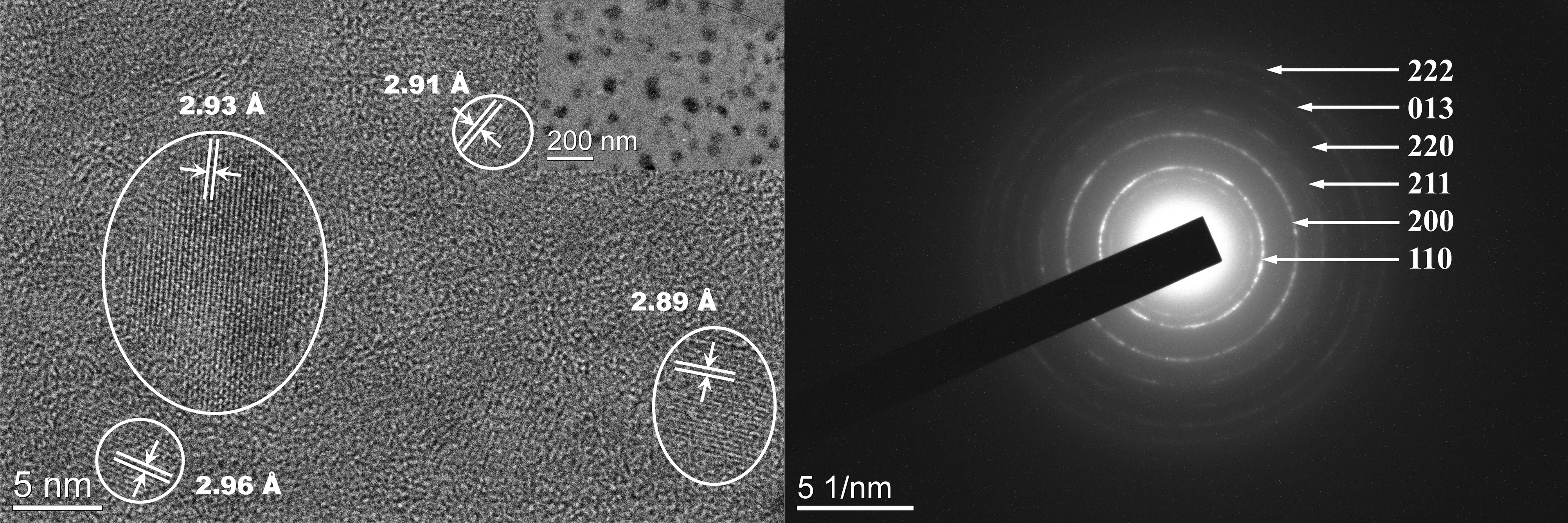
Among a large number of carbon phases which have been actively studied in the past few years (grafenes, fullerens, carbon nanotubes, diamonds) there is a rare С8 phase. This structural modification of carbon belongs to diamond-like phases and has the highest density among all carbon materials, which is 4.1g/cm3, which exceeds the density of diamond by 15%. After this phase was first discovered in 1979 (IPT, Kharkov) in carbon films during condensation of carbon plasma flows in vacuum, several studies on the synthesis of carbon quantum dots with C8 structure were held in the world. In our work we propose a new simple method of synthesizing cubic nanocrystals (NC) of С8 phase. During the carbonization of anthracene vapors, a carbon film gets deposited on a substrate, and 5–25 nm C8 lamellar nanocrystals are formed. The analysis of electronograms and electron microscopic images of direct lattice resolution proved the formation of C8 volume-centered cubic structure with 4.08 (0.02) Å unit cell parameter (Fig. 1). A hypothesis is proposed about the possibility of the formation of C8 nanocrystals in the vapor phase, which has been experimentally proved.
- N.S. Sukhinina, I.I. Khodos, A. Zhokhov, V.M. Masalov, I.I. Zverkova, S.S. Khasanov and G.A. Emelchenko.
A novel way of synthesising C8 cubic carbon nanocrystals
CrystEngComm, 2018, 20, 6133-6135, DOI: 10.1039/C8CE01225C
Theme 0032-2017-0002 Physics and technologies of new materials and structures
This work is a part of the research plan and state task of 2017Section II «Physical sciences».
Subsection 8 «Actual problems of condensed matter physics, including quantum macrophysics, mesoscopy, nanostructure physics, spintronics, superconductivity».
Programs of fundamental scientific research of state academies of sciences for 2013-2020.
Subsection 9 “Physical material science: new materials and structures including fullerens, nanotubes, grafenes and other nanomaterials and metamaterials (in physics and new functional material technologies for effective energy conversion)”
Programs of fundamental scientific research of state academies of sciences for 2013-2020.
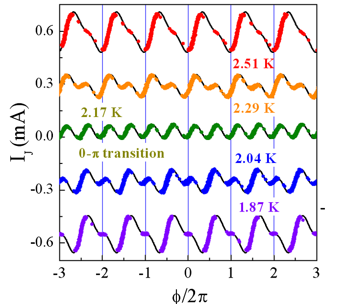
Monitoring of π-periodic phase-current relation in the Josephson junction with a ferromagnetic barrier
A. N. Rossolenko, V. V. Bolginov, V. A. Oboznov, D. S. Baranov, V. V. Ryazanov
In Josephson SFS contacts with a ferromagnetic (F) barrier at the point of transition to a state with an inverse difference in superconducting phases (π state), an anomalous “π-periodic” relation between the superconducting current and phase difference at the Josephson contact was observed in four different experiments [1].The discovered state corresponds to pair (4e) transport of superconducting (Cooper) electron pairs through the Josephson barrier. This fundamentally new topologically protected superconducting state can be used, for example, in topologically protected quantum computing systems. The observation of the new state became possible as a result of the substantial development of the technology for preparing Josephson SFS contacts in ISSP RAS [2].
- M.J.A.
Stoutimore, A.N. Rossolenko, V.V. Bolginov, V.A. Oboznov, A.Y.
Rusanov, D.S. Baranov, N. Pugach, S.M. Frolov, V.V. Ryazanov, and
D.J. Van Harlingen, Second-Harmonic Current-Phase Relation in
Josephson Junctions with Ferromagnetic Barriers,
Phys. Rev. Lett. 121, 177702 (2018). V.V. Bolginov, A.N. Rossolenko, A.B. Shkarin, V.A. Oboznov, V.V. Ryazanov, Fabrication of Optimized Superconducting Phase Inverters Based on Superconductor-Ferromagnet-Superconductor Junction.
Journ. Low Temp. Phys. 190 (5-6), 302 (2018).
Superconducting vortex core expansion into a diffuse normal metal in contact with a superconductor
O. Skryabina, V. Ryazanov
Vortices in superconducting systems exist due to macroscopic phase coherence. This work [1] proves both experimentally and theoretically that a quantized vortex with a clear, or normal core can exist in a relatively thick normal metal layer in contact with a superconductor. A vortex lattice was discovered on the surface of a copper layer 50 nm thick, deposited on a superconducting niobium, by means of scanning tunnel spectroscopy. The vortices have regular normal cores in the center, where the superconducting “mini-gap” placed in normal metal disappears. Normal layer cores are much larges than Abrikosov vortex cores in the niobium layer, due to the longer coherence of the superconducting pairs in normal copper.
A theoretical approach is introduced as well which describes a fully self-congruent pattern of vortex evolution distancing from the Cu/Nb interface, taking into account the interface resistance, applied magnetic field size and temperature. This work makes way for fine property tuning of superconducting vortices in hybrid structures.
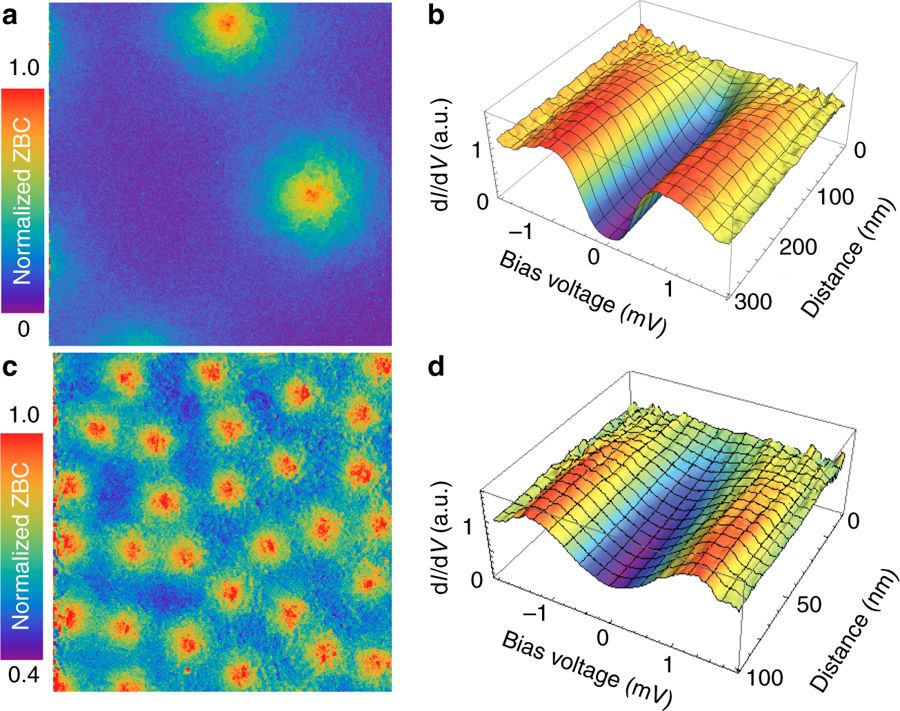
(b,d) radial evolution of tunnel conductivity spectra close to vortex cores.
The magnetic fields applied are same as in (a,c).
- V.S. Stolyarov et al, Nature Communications 9, 2277 (2018)
Random number quantum generator based on Poissonian statistics of photocounts with a rate of ≈ 100Mb/s
S.N. Molotkov
Experimental realization of a random number quantum generator is introduced. The primary source of randomness is a sequence of photocounts of a quazi single-photon radiation being registered by a matrix of silicon avalanche detectors - SiPM (Silicon Photo Multiplier). Using SiPM allows having tight control of the quantum character of the photocounts' Poisson statistics. A special algorithm of a nonexponential complexity allows getting all the randomness from the Poissonian process, that is, the random uniform sequence of 0 and 1.
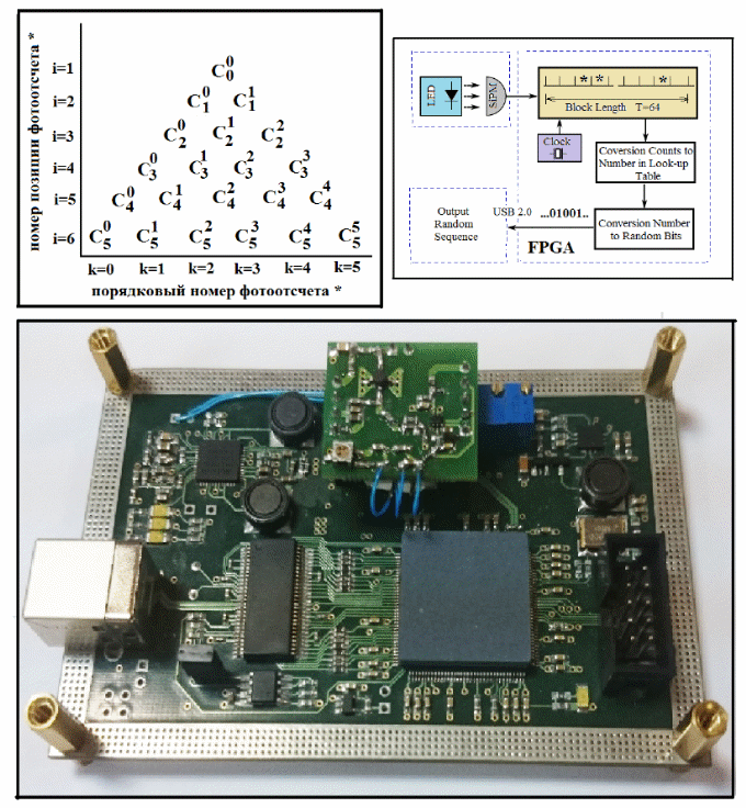
a) Table for numerating the photocount sequences that represents a well-known Pascal triangle (see main text for examples).
b) Functional circuit of random number quantum generator.
c) Its appearance.
Theme 0032-2017-0003 Coherent states and phase change in liquids and solids
This work is a part of the research plan and state task of 2017Section II “Physical sciences”
Subsection 8 «Actual problems of condensed matter physics, including quantummacrophysics, mesoscopy, nanostructure physics, spintronics, superconductivity»
Programs of fundamental scienctific research of state academies of sciences for 2013-2020.
Subsection 9 “Physical material science: new materials and structures including fullerens, nanotubes, grafenes and other nanomaterials and metamaterials (in physics and new functional material technologies for effective energy conversion)”. Programs of fundamental scienctific research of state academies of sciences for 2013-2020.
Subsection 12. “Contemporary problems of radiophysics and acoustics including fundamental basics of radio-physical and acoustical communicational methods, location and diagnostics, studying the nonlinear wave phenomena”.
Programs of fundamental scienctific research of state academies of sciences for 2013-2020
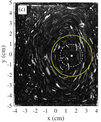
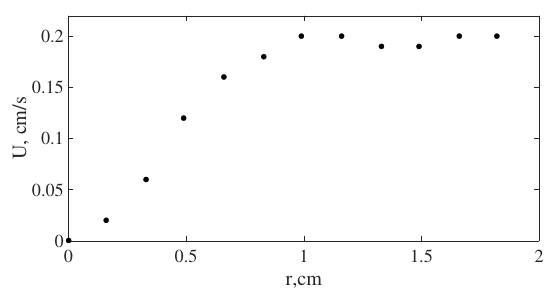
Structure of a coherent vortice of two-dimensional turbulence
M.Yu. Brazhnikov, A.A. Levchenko, A.V. Orlov
A pilot study was conducted on the formation of a coherent vortice in a turbulent current excited by a space-periodic electromagnetic force in a thin layer of a conductive liquid. Due to the two-dimensional turbulence reverse cascade, the current energy accumulates by scale comparable to the size of the experimental cell. A large-scale coherent vortice that occupies the most cell space gets formed. For the first time the radial profile of the coherent vortice's azimuth rate in its drifting center frame after switching off the energizing was determined. In the vortice core the azimuth rate increases linearly and reached its constant value beyond the vortice core. The coherent vortice's parameters from the pilot study correspond very well with theoretical predictions.
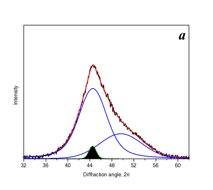
Renovation of amorphous nanocrystalline alloy structure by cryogenic treatment
A.S. Aronin, G.E. Abrosimova, N.A. Volkov, E.A. Pershina
In 2015 “Nature” published an article [1] about re-animation of an amorphous structure, and moreover, increasing its plasticity, being possible by means of cryothermal cycling.Nevertheless, there wasn't any study of those structures. Evolution of the amorphous phase of an aluminum-based structure (Al-Ni-Y, Al-Ni-Gd) under cryothermal cycling has been studied in ISSP RAS.
For the first time a restoration of an amorphous structure, as well as the decreasing of the fracture of a nanocrystalline structural component (if it was present before the cryothermal cycling) has been shown. Figure 1 shows the early section of the X-ray diagrams where the area corresponding to the crystalline part of the sample before (a) and after (b) the cryothermal cycling is hatched. It is shown that the using of cryothermal cycling, indeed, allows changing the structure of materials, including renovating of a partly-crystalline one, that helps making the material more flexible.
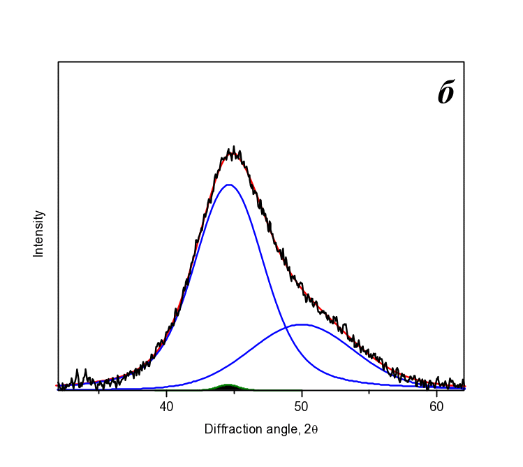
- Ketov S.V.; Sun, Y. H.; Nachum, Lu, Z, Checchi, A., Beraldin A. R., Bai, H.Y., Wang, W. H., Louzguine-Luzgin, D. V., Carpenter, M. A., Greer, A. L.
NATURE 524 (2015) N 7564, p. 200
Тheme 0032-2017-0004 Collective phenomena in electrone and exiton systems in semiconductor nanostructures
This work is a part of the research plan and state task of 2017Section II “Physical sciences”
Subsection 8 «Actual problems of condensed matter physics, including quantummacrophysics, mesoscopy, nanostructure physics, spintronics, superconductivity»
Manifestation of Fermi arcs in Andreev transport on the surface of Weyl semimetal
A.A. Kononov, S.V. Egorov, A.V. Timonina, N.N. Kolesnikov, E.V. Devyatov
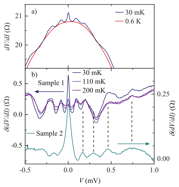
In topological semimetals the conductivity zone contacts the valence band at certain points (nodes) of the Brillouin zone. In a Weyl semimetal each Weyl node is characterized by certain chirality In k-space on the surface of the Weyl semimetal the Fermi-contours have the form of open arcs that connect the projections of the Weyl nodes onto the surface. Such exotic surface states are called Fermi arcs. We have made a research test of transport through the interface between a Weyl WTe2 semimetal and superconducting niobium. In the differential resistance spectra dV/dI (V) against the standart Andreev reflection nonperiodic resonances were discovered inside the superconducting Nb gap (see Figure). They emerge as Tomashev geometrical oscillations for the transport along topological surface state with an induced superconductivity near the Nb-WTe2 interface.
Observing clear geometrical resonances implies an allocated direction of charge movement in a surface state. It was theoretically predicted for Fermi arcs in Weyl semimetals.
See the full text in: EPL, 122, 27004 (2018)
DOI: 10.1209/0295-5075/122/27004
Control over some of the electron layers in field transistors with two-layered condycting channel
S.I. Dorozhkin, A.A. Kapustin, I.B. Fedorov
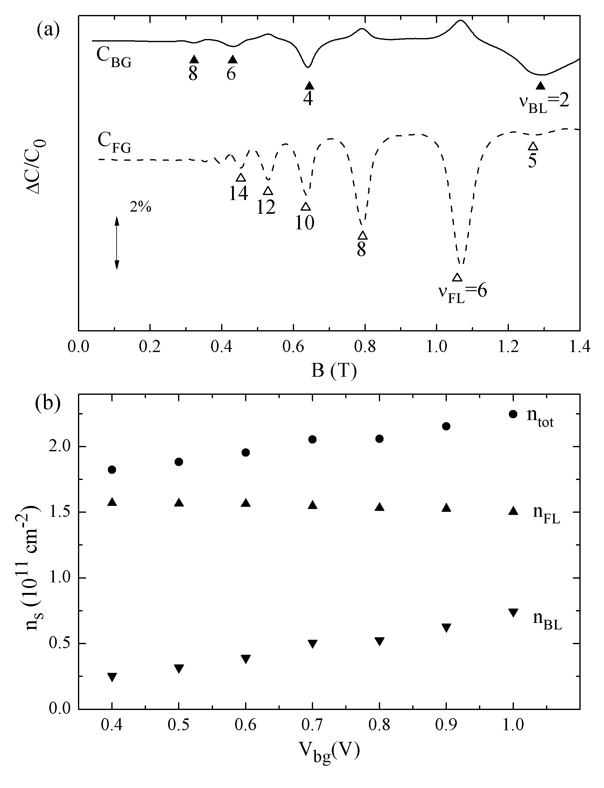
(a) Dependences of the volumes between the transistor conducting channel and the front (CFG) and back (CBG) shutters on the magnetic field. The marked minimums correspond to the filling of a whole number of Landau spin sublevels ν.
(b) Dependences of electron density in two diferent subzones of size quantization forming a two-layered system (nBL nFL), as well as of the full electron density ntot. on the voltage at the back shutter (Vbg).
Field transistors with high electron mobility (HEMT) that have non-standard architecture and two shutters, placed on different sides of the conducting transistor channel have been investigated. A new “volume” methodology has been developed for studying the properties of electron systems in the channel. It has been proved that this methodology allows measuring the compressibility of some separate electron layers in case of filling of two size quantization subzones in an asymmetrical quantum well realizing the conducting channel, as well as defining the electron density in each of the layers.
S.I. Dorozhkin, A.A. Kapustin, I.B. Fedorov, V. Umansky, K. von Klitzing and J.H. Smet “Characterization of individual layers in a bilayer electron system produced in a wide quantum well”.
Journal of Applied Physics 123, 084301 (2018).
Local impedance on a rough surface of a chiral p-wave superconductor
A.F. Shevchun, M.P. Trunin
One of a most interesting trends in contemporary solid state physics is investigating the properties of non-traditional and topological superconductors.
Superconductivity in the Sr2RuO4 material proved to be unique. Measurments have been held of surface impedance in Sr2RuO4monocrystals in a broad bandwidth from 9 to 42 GHz, which show non-typical properties of this material in superconducting state. That is, small changes in absorbtion of MMW radiation during transition from normal to superconducting state, and non-typical temperature dependence of the imaginary impedance part. A self-congruent approach was developed for calculating the local impedance of a rough surface of a chiral p-wave superconductor. By using the quazi-classical formalism of Eilenberger-Larkin-Ovchinnikov, we calculated the pair potential, the mating function and the surface state density with the diffusing electron scattering on the surface taken into account.
Qualitatively, the features of Sr2RuO4can be explained within the framework of chiral p-wave triplet mating and odd frequency superconductivity emerging on the surface.
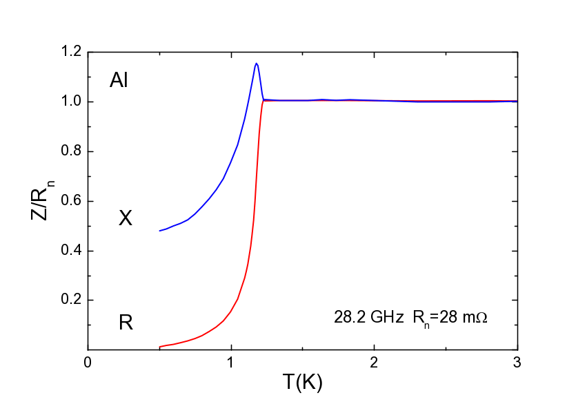
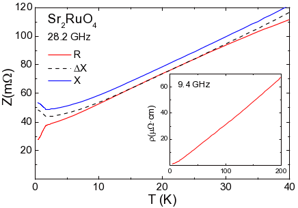
- S. V. Bakurskiy, Ya. V. Fominov, A. F. Shevchun, Y. Asano, Y. Tanaka,
M. Yu. Kupriyanov, A. A. Golubov, M. R. Trunin, H. Kashiwaya, S.
Kashiwaya, and Y. Maeno, Local impedance on a rough surface of a
chiral p-wave superconductor,
Phys. Rev. B98, 134508 (2018)
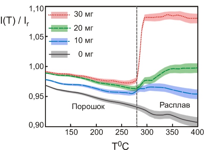
Mechanism of domain structure dynamics of spontaneous electric field in a lossless state induced by MMW radiation
S.I. Dorozhkin
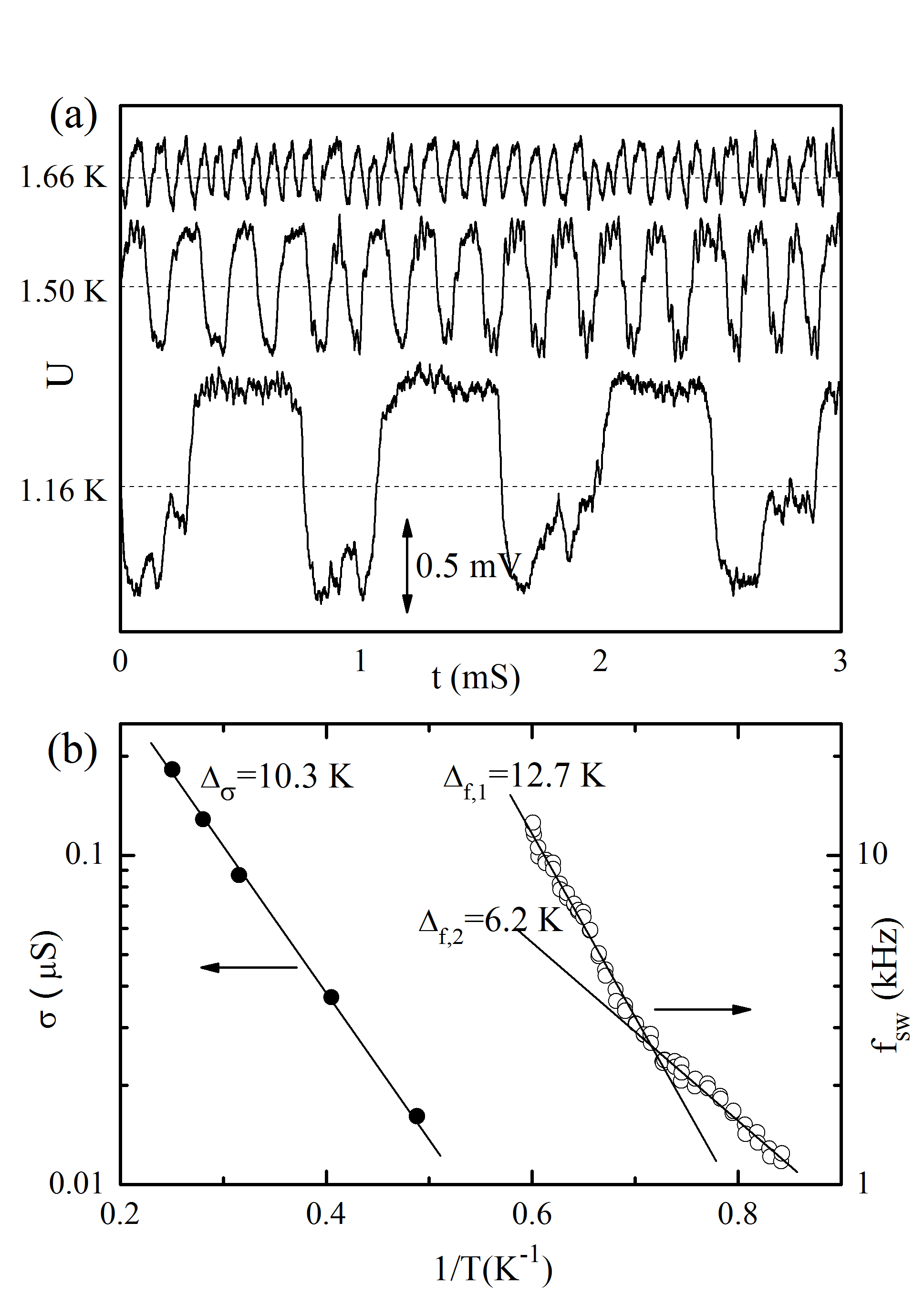
(a) Switching sygnals of MMW photo-electromotive force exposed under 47 HGz radiation at three different temperatures indicated near the curves.
(b) Dependance of the switching frequency (open symbols, scale on the right) and conductivity of the doping layer (closed symbols, scale on the left) on temperature.
The aquired results testify that the spontaneous electric field domain structure dynamics that emerges in an non-dissipating state induced by MMW radiation (called “zero-resistance state” in English resources) that we discovered and measured is conditioned by the screening of the field by selective doping layer charges, that is the inevitable part of contemporary semiconductor structures with high-mobility two-dimensional electron systems. We have found that the switching frequency of the spontaneous electric field and the conductivity of the doping layer depend on temperature in a thermally-activated manner (by Arrenius law) with close values of activation energy. This proves these values are proportional, which is the key moment of the screening model.
- S.I.
Dorozhkin, V. Umansky, K. von Klitzing and J.H. Smet. Freezing the
spontaneous electric field domains in MMW-induced states with low
dissipation.
JETP Letters, 108, 217-222 (2018). - S.I. Dorozhkin, V. Umansky, K. von Klitzing and J.H. Smet. The
dynamics of spontaneous electric field in two-dimensional electron
system under MMW radiation, and the donor layer.
JETP Letters, 107, 68-72 (2018).
Abnormally strong decay reduction of plasmon excitations in two-dimensional electron disks
P.A. Gusikhin, V.M. Muravyov, A.A. Zagitova, I.V. Kukushkin
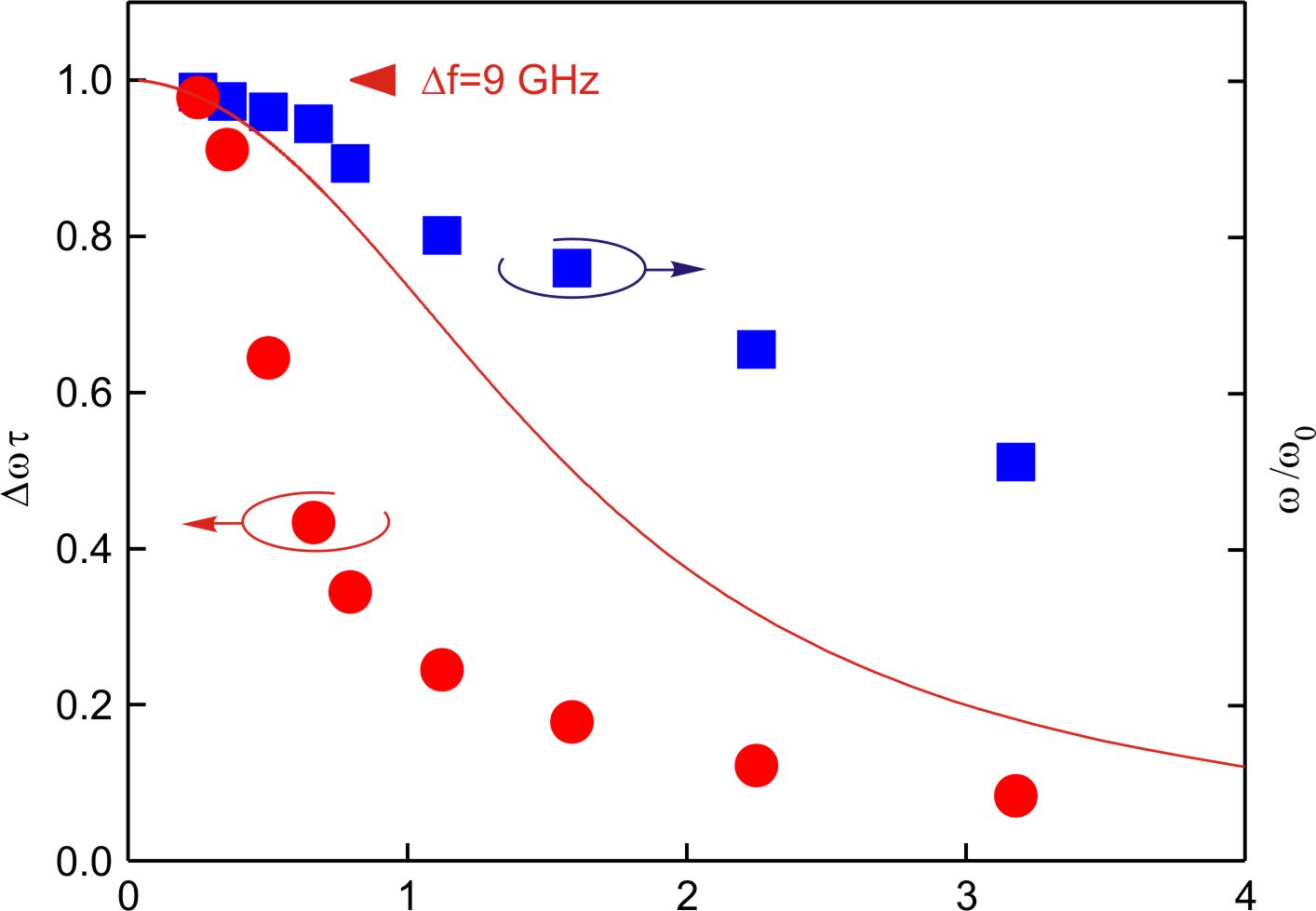
Experiments held in the Laboratory of Non-equilibrium Electronic Processes of ISSP RAS were the first to show the decay of plasmon excitations in in a significant delay mode. It has been discovered that plasma wave decay in this mode happens to be abnormally suppressed, despite the former notion that a plasmon resonance significantly broadens due to the radiation input in plasmon decay. It has been determined that the dependence of a plasmon resonance's normalized width Δωτ on time-delay parameter A has a universal character. This law has been tested on three different structures with concentration values of 0.8×10¹¹, 3.9×10¹¹ and 6×1011 cm-2, and the reverse transport scattering time values of 3.4×10¹⁰ and 5.6×10¹⁰s-1. It is shown that in a significant delay mode the plasma waves are weakly decaying up to room temperature. That gives numerous opportunities for creating effective terahertz radiation detectors working at room temperature.
The experimental results were published in Physical Review Letters 121, 176804 (2018).
Innovational achievments of 2018
approvedby ISSP RAS Academic Board on December, 10, 2018(protocol №30)
Subsection9. “Physical material science: new materials and structures including fullerens, nanotubes, grafenes and other nanomaterials and metamaterials (in physics and new functional material technologies for effective energy conversion)”
Programs of fundamental scientific research of state academies of sciences for 2013-2020.
Luminophor for LEDs
S.Z. Shmurak, V.V. Kedrov, A.P. Kiselev, T.N. Fursova
In RE1-x-yCexTbyBO3, где RE – Lu, Gd, Yt samples the ion glow Tb3+ is observed at sample excitation in Се3+ ion absorption band. This proves non-emissive transfer of electron-beam excitation enegry from Се3+ to Tb3+ions due to Coulomb dipole-dipole interaction between these ions. The glow intensity of Tb3+ at excitation in a Ce absorption band is higher than that of an industrial luminophor Y2O2S(Tb), and its glow intensity is ~10 times higher than the Tb3+ glow in the most intensively excited excitation band in Tb3+ ion (λmax = 236 nm). This is due to the high energy transfer effectiveness from Се3+ions to Tb3+that has been experimentally determined, its value being ~ 85%. It is shown that the Tb3+ions excitation spectrum can be deliberately displaced in the range from 339 to 367 nm, the Lu1-x-yCexTbyBO3, its structural state being changed ‑ to the glowing region of industrial GaN light emitting diodes.
Considering the high glowing intensity, radioactive and chemical proof of borates, the high thermal conduction, as well as the possibility of directing its excitation spectrum change, Lu1-x-yCexTbyBO3 composition can be seen as an effective green-emitting luminophor for light emitting diodes.
- S.Z. Shmurak, , V. V. Kedrov, A. P. Kiselev, T. N. Fursova, and O. G. Rybchenko. «Energy Transfer from Ce3+ to Tb3+ in Yttrium and Gadolinium Orthoborates Obtained by Hydrothermal Synthesis».
Physics of the Solid State, 2018, Vol. 60, No. 12.
BSCCO monocrystals for THz-emitters
A.B. Kulakov
Efforts on developing the technology of growing Bi2Sr2CaCu2O8 (BSCCO) monocrystals and their subsequent fragmentation and annealing have been taken for four years in ISSP RAS. At the same time, a group leaded by A.L. Pankratov (Institute for Physics of Microstructures, RAS, Nizhny Novgorod) terahertz range emitters based on BSCCO monocrystals have been developed. The technology developed at the Institute for Physics of Microstructures makes possible the making of mesas 0.5 cm in diameter that can emit at a frequency of 0.8 THz [1]. See volt-ampere curves for a BSCCO mesa in Fig. 1. BSCCO crystals provided by ISSP RAS are an integral part of this technology. These results prove the quality of our BSCCO crystals. Currently, our Institute is the only place in Russia where these crystals are produced. If we can reduce the concentration of planar defects by 5 times, our crystals will become attractive for investors.
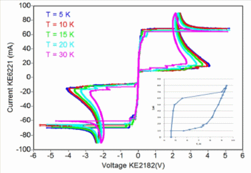
- L.S. Revin, E.A. Vopilkin, A.L. Pankratov, S.A. Kraev, A.A. Yablokov,
A.B. Kulakov. Fast technology for fabrication of thick single
Bi2Sr2CaCu2O8+x mesas
on a Cu substrate/.
Supercond. Sci. Technol. 31(2018)104001(5pp). DOI: 10.1088/1361-6668/aada8.
Layered composites with a metal matrix reinforced with oxide fibers aquired by a modification of the Stepanov method
V.M. Kiyko
Lab flow charts and modes of diffusion bonding for producing fiber-laminated composites with oxide fiber and matrices based on titanium, niobium and molybdenum have been set up. Sapphire, yttrium-aluminum-garnet and eutectic (sapphire-yttrium-aluminum-garnet) fibers have been produced and tested out. Relationship between their length and endurance has been measured. Their endurance reaches 4000 MPa at lengths equal to tenfold fiber diameter. Pilot samples of composites including sapphire fibers and matrices based on titanium and niobium have been produced and tested. For samples that contain a titanium-based matrix a dependency of the composites' endurance on temperature in the range from 20oC to 900oC has been measured, its maximum reached at 700oC.
Development of technology and facilities for producing profiled articles from resistance metals by 3D printing
D.N. Borisenko, A.A. Zhohov, E.B. Borisenko
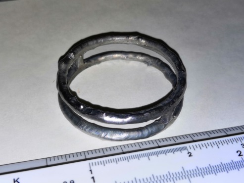
The method of producing profiled articles from resistance metals is realized by applying the metal layer-by-layer in the manner of local encrusting (sculling) arc melting. Electric arc power supplies for various welding atmospheres (argon, helium, hydrogen) have been developed and tested. By means of controlled pinch-effect the task of generating and stabilizing the plasma channel of a high-pressure arc at random scan profile of the electrode has been solved. A patent application for “Electrode for arc melting of metals” has been filed. During the experimental production of molybdenum crucibles it was shown that the printing speed by means of local encrusting arc melting exceeded by ten folds that of selective laser melting.
At the next stage the original facility for superfine powder supply into the melting zone for non-stop material welding was developed and produced. A patent application for “Screw dozer for resistance metal powders” was filed. Be means of the facility a molybdenum heating element for an induction furnace has been made (see Fig.1).
While studying the microstructure and qualities of the aquired material it became clear that the pore volume after a double immersion into a hot-dip bath was close to zero. The remaining occasional pores contained micron-size whiskers.
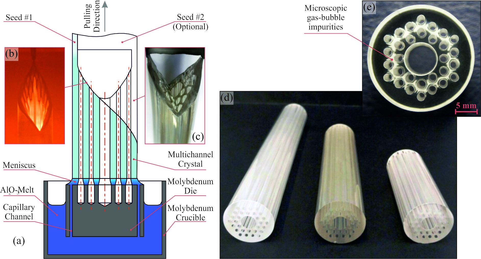
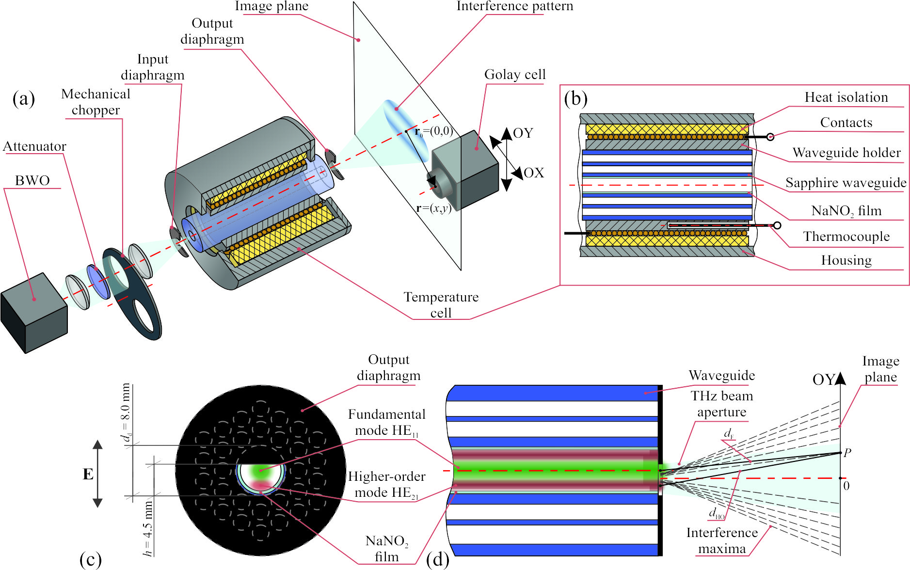
Sapphire waveguide for THz intra-waveguide spectroscopy and interferometry in hostile environment
G.M. Katyba, I.A. Shikuniva, I.N. Dolganova, V.N. Kurlov
Methods of high-temperature terahertz intra-waveguide spectroscopy and interferometry using a multi-channel profiled sapphire crystal that works as a THz waveguide and a cell for the substance investigated at the same time has been developed. By means of computational electrodynamic methods a numerical calculation of a waveguide section geometry was conducted aiming at optimizing the dispersion and loss during the THz radiation transmission in a single-mode operation, or providing the the estimated quantity and quality of waveguide modes for realizing interferential measurement principles. A THz waveguide with a single central channel and two rows of photocrystalline (PC) envelope channels has been calculated that provided high terahertz quality (i. e. low dispersion and loss) in a broad spectral band from 0.2 to 1.2 THz in a dual-mode operation. This is due to the fundamental mode and one of the higher modes having the lowest loss rates that are comparable to each other in value.
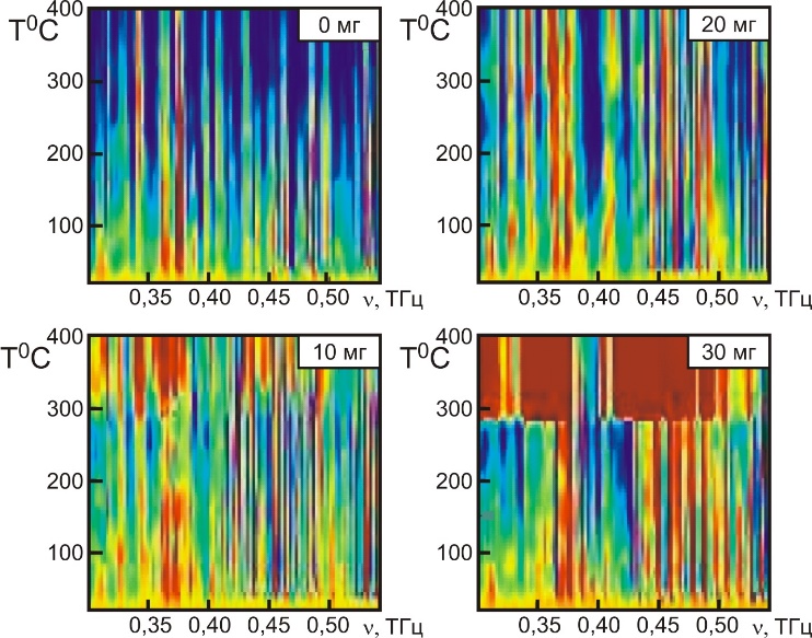
The developed and manufactured sample of the PC THz waveguide (see Figure 1) was studied using numerical and natural experiments to prove its technical capacity that had been calculated during computer modelling. The experimental studies of the waveguide were realized using the THz impulse spectroscopy methods, i. e. dispersion estimation and spectral waveguide mode loss, as well as THz mode imaging methods, i. e. visualization of waveguide modes and their interference in a profiled crystal section being exited by a constant THz radiation. To demonstrate the high-temperature THz intra-waveguide spectroscopy in the frequency range, and the THz waveguide interferometry using the developed sapphire waveguide, experimental measurements of the phase changes of small amounts of NaNO2powder introduced into the waveguide have been held.
Figure 2. The high sensibility of the system developed is shown.
Figure 3. Due to combining the capabilities of the method of acquiring the profiled sapphire crystals with its unique qualities, the waveguide developed can be used for THz high-accuracy spectroscopic measurements in hostile environment at temperatures up to 1850⁰C.
Chemical Mechanical treatment of metal articles
N.V. Klassen, E.N. Klassen, N.P. Kobelev, E.L. Kolyvanov
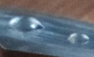
A technology of chemical mechanical treatment of metal articles is patented which is based on a new way of deep incorporation of alloying elements, nanoparticles, or organic molecules into subsurface layers of metal articles by local dynamic deforming of the surface with a rolling ball, and at the same time applying the materials that are being incorporated. This technology allows express strengthening, anti-corrosion and anti-icing protection of load-bearing structures, pipelines (including weld seam protection), power lines, etc., directly on site in the field or under water. The work was done within the international project together with the Institute of Technical Acoustics, NASB (National Academy of Sciences of the Republic of Belarus).
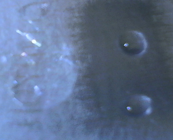
On the left is a puddle of water wetting the surface of an aluminum plate. On the right the same drop of water does not make a puddle or wet the same aluminum surface that has been chemically and mechanically treated with ball rolling, a water-repellent organic matter incorporated deeply into it.
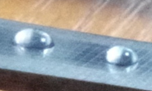
The result of incorporating carbon nanoparticles into an optically transparent cesium iodide crystal is shown. The surface being treated is shown above. Rolling time is 5 minutes, carbon incorporation depth is 50 mkm.