
")
")


Main achievements in 2019 (based on state order)
approved by ISSP RAS Academic Board on December, 9, 2019 (protocol № 27)
Section II «Physical Sciences», Subsection 9
Electric arc 3D printing of refractory metal products
D.N. Borisenko, E.B. Borisenko, A.A. Zhokhov, B.S. Red’kin, N.N. Kolesnikov
Original device has been developed, and the principal possibility is shown of manufacturing profiled products from refractory metals by 3D printing using an electric arc in protective gas atmosphere.
The offered additive method is realized by layer-by-layer deposition of metal of a local encrusting electric arc melting type.
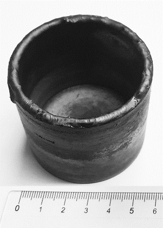
Experimental production of molybdenum crucibles shows that the printing speed is by two or three orders of magnitude higher than the printing speed of selective laser sintering.
Examples of the resulting products are shown in the photographs.
 |
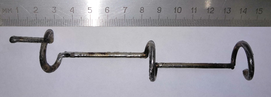 |
| Molybdenum crucible | Tungsten collinear electrode for SHF plasma generation and welding of metals in protective gas atmosphere |
Articles:
- D.N. Borisenko, E.B. Borisenko, A.A. Zhokhov, B.S. Red’kin, N.N. Kolesnikov. Equipment and method of manufacturing profiled products from refractory metals by 3D printing method. Experimental Appliances and Techniques , 2019, No. 6, pp. 112-116. DOI: 10.1134/S0032816219050185 (in Russian)
- Borisenko D.N., Kolesnikov N.N. Electrode for arc melting of metals. Patent for an invention № 2682553, published on 9.03.2019, Bull. № 8.
- D.N. Borisenko, A.A. Zhokhov, S.P. Maistrenko, A.M. Khamidov. A screw doser for refractory metal powders. Patent for an invention № 2701277, published on 25.09.2019, Bull. № 27
Section II «Physical Sciences», subsection 8
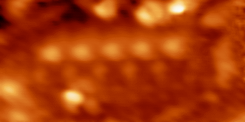
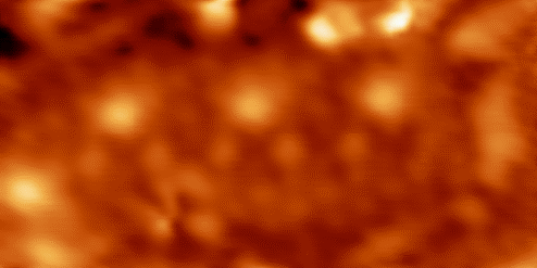
Surface modification of MoO2+x/Mo(110) induced by a local electric potential
S.I. Bozhko, Natalia Tulina, Vladimir Bozhko et al.
Surface modification of MoO2+x/Mo(110) induced by a scanning tunnelling microscope tip local electric potential is researched.
Applying a voltage pulse to the tunnelling microscope tip results in the removal of a cluster of oxygen atoms from the surface.
The cluster size is determined by the applied voltage magnitude, and the distance between the STM tip and the surface.
Atoms are removed from the surface only when negative voltage was applied to the STM tip.
With such voltage polarity the force acting on the negatively charged oxygen adatom is directed along the normal to the surface and presses it against the surface.
At a certain threshold voltage, it is possible to remove single adatoms located 0.5nm apart from each other from the surface.
In the Figure on the left, green arrows indicate the location of the electric field pulses applied. In the Figure on the right, blue arrows indicate the result of electric field application.
Dependence of threshold voltage from the distance between the STM tip and the surface shows a kink at the distance where the tunnel current turns to 0.
Based on model calculations of the MoO2+x/Mo(110) structure in the density functional theory approximation, a mechanism of surface modification by the electric field of STM tip is proposed, which lies in adatom penetration into the sample volume.
The potential barrier to be overcome during penetration into the near-surface layer is estimated.
The value obtained is in good agreement with the potential barrier for electrodiffusion of oxygen atoms.
Oxygen atoms removal from the surface occurs when an electric field of ~107 V/cm is applied, which is consistent with the value of the threshold electric field of memristor switching in MoO2.
Related article:
Sergey I. Bozhko, Killian Walshe, Natalia Tulina, Brian Walls, Olaf Lübben,
Barry E. Murphy, Vladimir Bozhko, Igor V. Shvets, «Surface
modification on MoO2+x/Mo(110) induced by a local electric
potential», Scientific Reports (2019) 9, 1-11.
DOI: 10.1038/s41598-019-42536-9
Section II «Physical sciences», Subsection 8
Amorphisation of partially-crystalline structure under voltages conditioned by cryogenic heat treatment
G.E. Abrosimova, A.S. Aronin, N.A. Volkov, E.A. Pershina
Renovation of amorphous structure in amorphous nanocrystalline samples under cryogenic heat treatment is studied.
It is shown that the renovation of an amorphous structure does not depend on whether the nanocrystals in their amorphous phase are formed by demormation or thermally.
Voltages of dislocation generation and voltages conditioned by thermal gradients between neighboring areas in a heterogenous structure due to varying thermal-expansion coefficients (CTE) is calculated.
It is found that the voltage within Al nano-crystals in a Al87Ni8Gd5 alloy at temperature variation from 77 to 393 К rises up to 90 mPа.
The cryogenic treatment under repeated stress caused by voltage growth that occurs when the thermal-expansion coefficients (CTE) vary and the stress limit decreases can lead to deformative amorphization.
 |
 |
 |
 |
 |
 |
Related article:
G. Abrosimova, N. Volkov, Tran Van Tuan, E. Pershina, A. Aronin
«Cryogenic rejuvenation of Al-based amorphous-nanocrystalline
alloys», Mater. Let. 240 (2019) 150-152
DOI: 10.1016/j.matlet.2018.12.131
Section II “Physical sciences”, Subsection 9
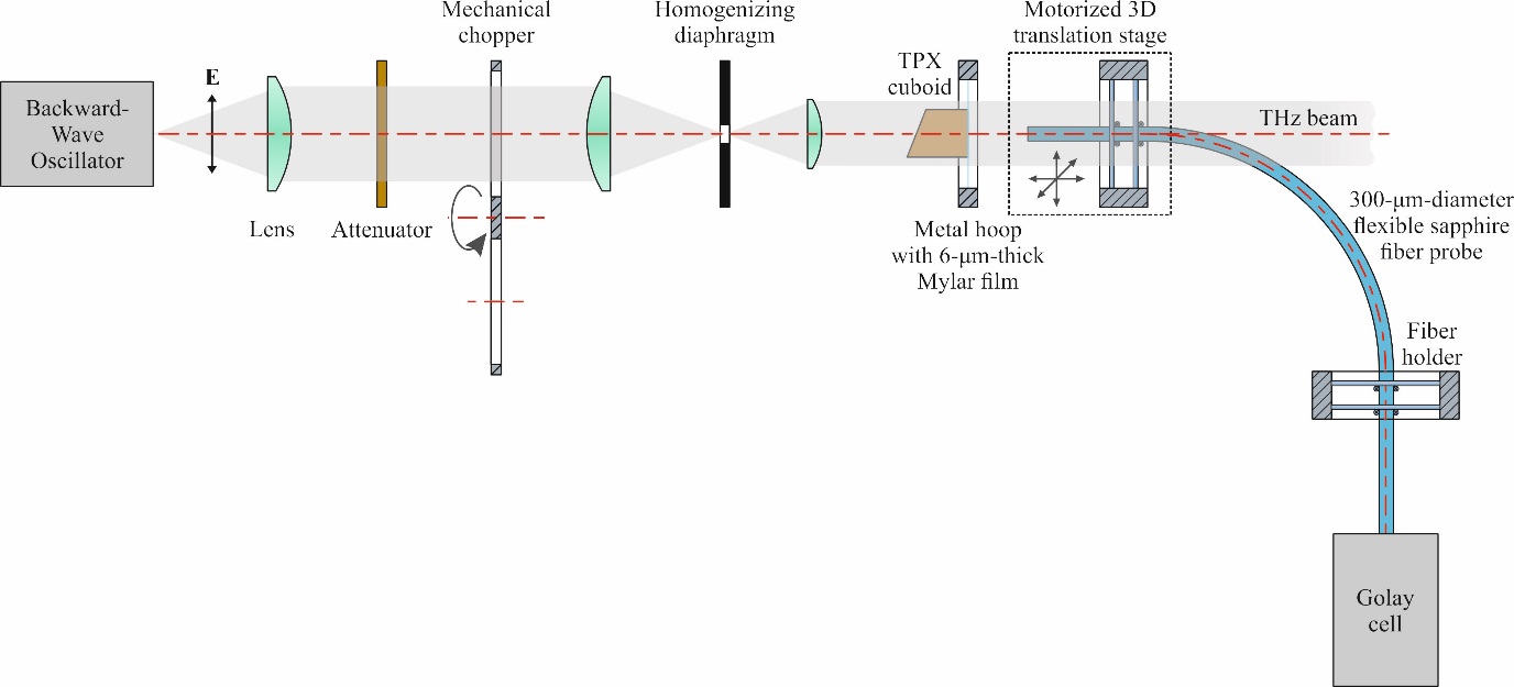
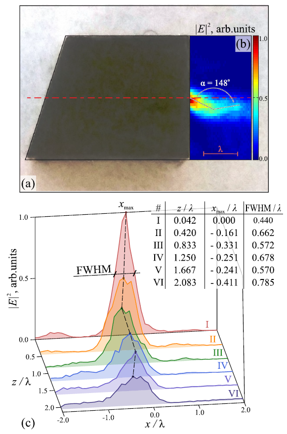
Experimental observation of a photonic hook
G.M. Katyba, I.N. Dolganova, V.N. Kurlov et al.
A method of THz probe microscope scanning based on flexible sapphire fibers used as probes is created.
High values of refraction within THz range and, consequently, significant localization of waveguide mode in a sapphire fiber provides sub-wave spatial resolution of the THz visualization (see Figure 1).
The first experimental observation of the so-called photonic hook (PH), a new type of a photonic jet with a caustic curve (see Figure 2) was formed on the back side of a dielectric prism, its size comparable to that of a falling emission wavelength.
A sapphire fiber 300 mkm in diameter with system resolution of 0.25 λ is used as a scanning probe.
The curve radius of the observed PH is less than the wavelength, the minimal size of the constriction is 0.44 λ.
The observed effect is of potential interest for optics and photonics, particularly for microscopy with ultra-small resolution, as a base for creating an optical tweezer for micro- and nano-sized objects.

Related article:
Minin I.V., Minin O.V., Katyba G.M., Chernomyrdin N.V., Kurlov V.N.,
Zaytsev K.I. “Experimental observation of a photonic hook” -
Applied Physics Letters, 2019, v.114, 031105.
DOI: 10.1063/1.5065899
Section II “Physical Sciences”, Subsection 8
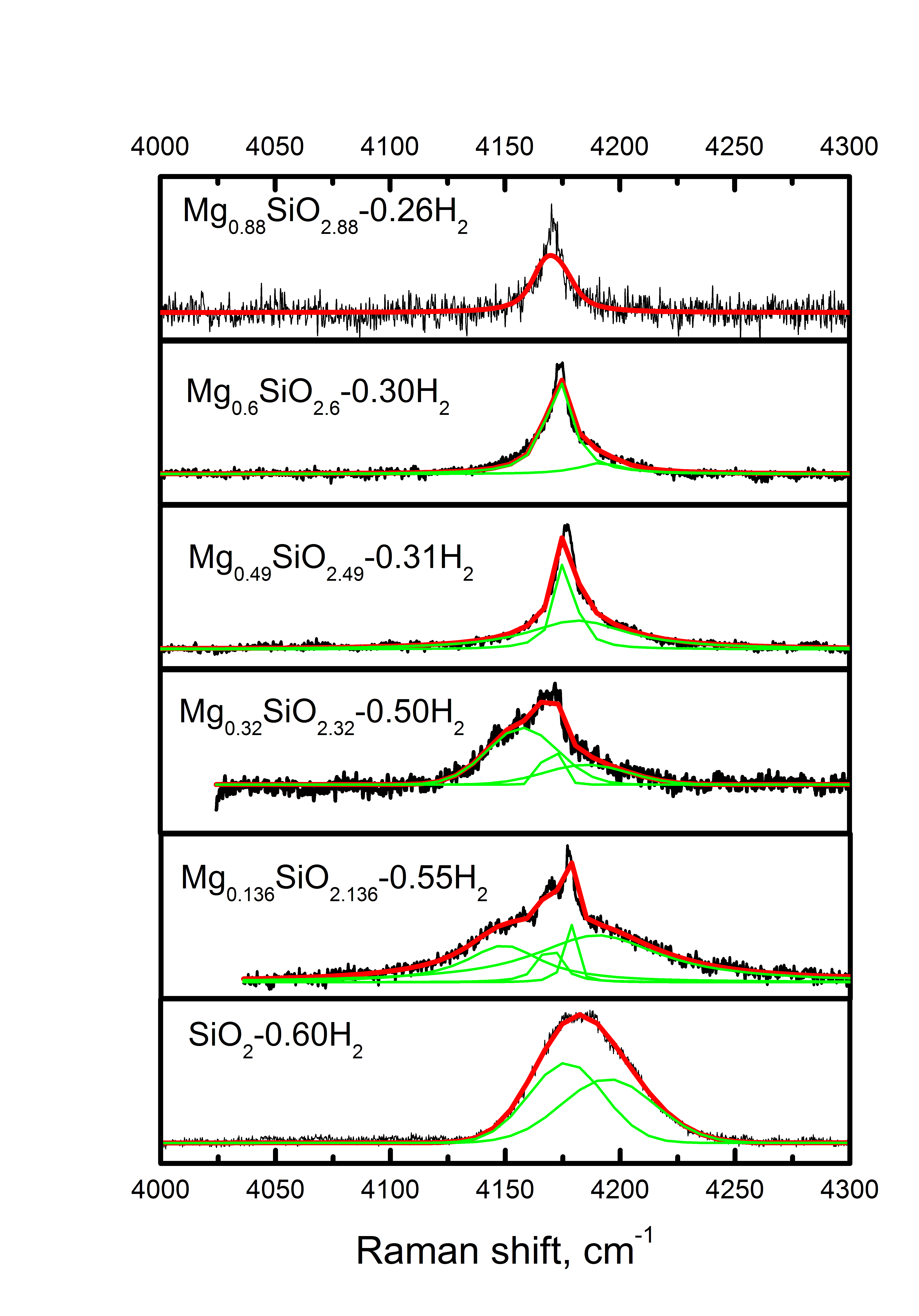
Solid solutions of molecular hydrogen in amorphous magnesium silicate
V.S. Efimchenko, N.V. Barkovsky, V.K. Fedotov, K.P. Meletov, S.V. Simonov, S.S. Khasanov, K.I. Khryapin
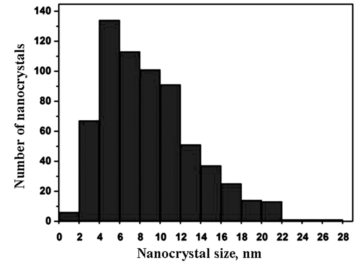
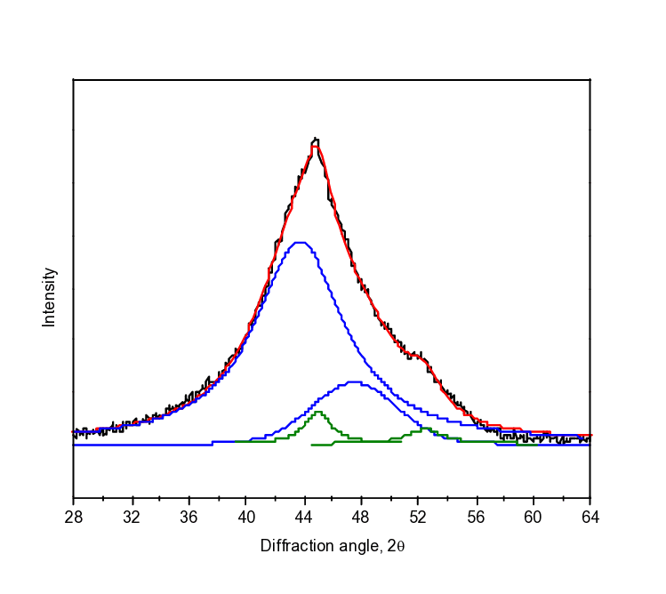
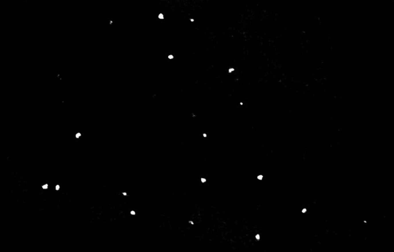
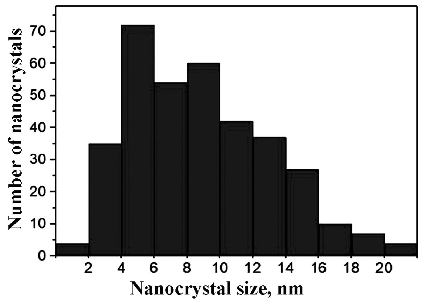
Large-mass samples of solid solutions of molecular hydrogen in amorphous magnesium silicate MgySiO2+y (y = 0–0.88) are prepared at hydrogen pressure of 75 kbar and temperature of 250 °C, tempered up to liquid nitrogen temperature for the first time.
The tempered samples are studied at atmosphere pressure by the methods of thermodesorption, X-ray diffraction and Raman scattering spectroscopy.
All the samples remained amorphous after hydration, the samples with y≥0.32 consolidating irreversibly.
In the Raman scattering spectra (see Fig. 1) gradual narrowing of expanding H-H hydrogen oscillations is discovered at growing quantities of magnesium cations.
The obtained result does not correlate with the overall hydrogen content in the samples, as well as with the irreversible consolidation of the amorphous magnesium silicate lattice.
The difference may be due to the different structuring of the initial amorphous silicates that are similar to silica glass (SiO2) at low concentrations of magnesium, and enstatite glass (MgSiO3) at high concentrations.
Therefore, the Raman scattering spectra of hydrogen dissolved in amorphous silicate matrix can indicate its structure.
Related article:
Vadim S. Efimchenko, Nikolay V. Barkovskii, Vladimir K. Fedotov, Konstantin
P. Meletov, Sergey V. Simonov, Salavat S. Khasanov, Kirill I.
Khryapin «High-pressure solid solutions of molecular hydrogen in
amorphous magnesium silicates» J. Alloys Comp. 770 (2019)
229-235.
DOI: 10.1016/j.jallcom.2018.08.111
Section II “Physical Sciences”, Subsection 9
Properties of electron systems in field transistors with a double quantum well
A.A. Kapustin, S.I. Dorozhkin, I.B. Fedorov et al.
Investigations are performed of field transistors with high electron mobility (HEMT) that have non-standart architecture, two conducting channels located in two close GaAs quantum wells and two gates located on different sides of the conducting transistor channels.
For such transistors a new capacitance research method of separate electron layers located in different quantum wells is developed.
Equations are obtained for capacitances measured between different gates and the electron system that make allowance for quantum corrections related to electron compressibility in different layers.
In the zero and the quantizing magnetic fields manifestations of negative values of compressibility of a two-dimension low density electron system are discovered.
Significant spread-out of areas where non-compressible phases on the filling factors of spin-resolved Landau 2 and 1 levels along the magnetic field is discovered in the layer with a higher density. The spread-out is caused by the filling of the second layer.
Estimations are made of the steps in chemical potential for the corresponding quantum Hall effect conditions.
Related article:
A.A. Kapustin, S.I. Dorozhkin, I.B. Fedotov, V. Umansky, Yu. Kh. Smet.
Quantum effects in field transistor capacitance with a double quantum
well. JETP Letters 110, 407-413
(2019).
DOI: 10.1134/S0370274X191
Section II “Physical Sciences”, Subsection 12
Vortices on the surface of normal helium He-I formed by heat-gravitational Rayleigh-Bénard convection in the volume of liquid layer
A.A. Pel’menev, A.A. Levchenko, L.P. Mezhov-Deglin
It is found experimentally that heat-gravitational Rayleigh-Bénard convection emerges in the volume of normal helium He-I layer when it is heated from above in a immobile vessel at temperatures close to T_. The convection is accompanied by vortice generation on the free surface of He-I.
The interaction of the vortices with one another and with the vertical vortice structures formed in the volume of the layer during the emergence of turbulent Rayleigh-Bénard convection leads to emergence of large-scale vortices (vortex doublet) on the surface.
The Rayleigh-Bénard convection in the layer volume fades fast over time when the liquid layer is heated over 2.3 K.
The maximum energy values in large-scale vortices on the surface Emax in k-space decrease proportionally to Emax ∼ t−1 over time under no exitation and within the temperature interval of T = 2.6−3.3K.
Related article:
A.A.
Pel’menev, A.A. Levchenko, L.P. Mezhov-Deglin. Vortices
on the surface of normal helium He-I formed by by
heat-gravitational Rayleigh-Bénard
convection in the volume of liquid layer.
JETP Letters 110, Issue 8, pp. 545–550 (2019) (in
Russian).
DOI: 10.1134/S0370274X19200062
Section II “Physical Sciences”, Subsection 8
Proton conductance of water in mesoporous materials
I.A. Ryzhkin, M.I. Ryzhkin, E.A. Galitskaya, V.V. Sinitsin
A theoretical model explaining high proton conductivity of water in mesoporous materials is proposed. The proton conductivity of water confined in nanochannels is six or seven orders of magnitude higher than the value for bulk water.
The key concept of the model lies in topological inconsistency of the ice rules with ordering of interface molecules caused by interaction of water molecules with the confining walls.
Numerical estimates within our model are in quantitative agreement with the measured proton conductivities of nanoporous materials with different chemical compositions, degrees of crystallinity, and structure morphologies.
The model gives a useful scheme for producing nanoporous materials with high proton conductivity.
Related article:
I.A. Ryzhkin, M.I. Ryzhkin, A.M. Kashin, E.A. Galitskaya, V.V. Sinitsyn.
High proton conductivity state of water in nanoporous materials, EPL
126, 36003 (2019)
DOI: 10.1209/0295-5075/126/36003
Section II “Physical Sciences”, Subsection 8
Quantum phase transition in ultrahigh mobility SiGe/Si/SiGe two-dimensional electron system
M.Yu. Melnikov, A.A. Shashkin, V.T. Dolgopolov et al.
The metal-insulator transition (MIT) is an exceptional test bed for studying strong electron correlations in two dimensions in the presence of disorder. In the present study, it is found that in contrast to previous experiments on lower mobility samples, in ultrahigh mobility SiGe/Si/SiGe quantum wells the critical electron density nc of the MIT becomes smaller than the density nm, where the effective mass at the Fermi level tends to diverge. nc < nm shows that the two densities are not connected directly in least disordered electron systems at any rate. Near the topological phase transition expected at nm, the metallic temperature dependence of the voltage should be strengthened, which is consistent with the experimental observation of more than an order of magnitude higher resistance drop value with temperature decreasing below ∼1 K.
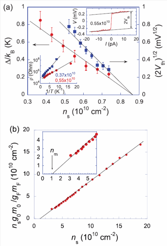
(b) Dependence of effective mass on Fermi edge mF from the electron density. The solid line indicates linear approximation. The insert shows an enlarged view of the dependence at low electron densities where nm = 1.1 ± 0.1 × 1010 cm−2.
Related article:
M.Yu. Melnikov, A.A. Shashkin, V.T. Dolgopolov, Amy Y.X. Zhu, S.V.
Kravchenko, S.-H. Huang, C.W. Liu «Quantum
phase transition in ultrahigh mobility SiGe/Si/SiGe two-dimensional
electron system», Phys. Rev. B 99, 081106(R)
(2019).
DOI: 10.1103/PhysRevB.99.081106
ection
II “Physical Sciences”, Subsection 8, Theme 0032-2019-0012
“Coherent states and phase change in solid and liquid-state bodies”
Superconductivity in lanthanum hydride at 250 K and high pressures
M.A. Kuzovnikov et al.
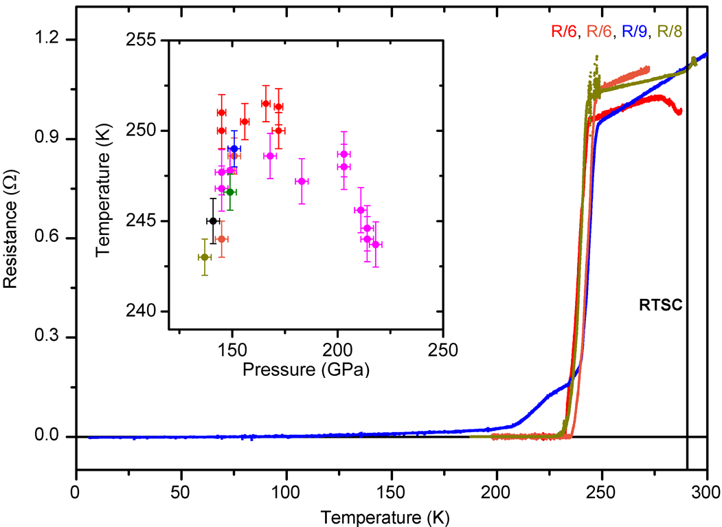
First-principle calculations based on density functional theory suggest a new family of superconducting poly- or super-hydrides with a clathrate-like structure in which the host atom (calcium, yttrium, lanthanum) is at the centre of a cage formed by hydrogen atoms.
For LaH10 and YH10, the superconducting transition is predicted to occur at critical temperatures between 240 and 320 kelvin at megabar pressures. In our study we present a hydrid LaH10 experimentally obtained with a critical temperature of Tc ≈ 250 K at a pressure of about 170 gigapascals (see Figure 1). Superconductivity is evidenced by the observation of zero resistance, isotopic dependence Tc (The LaD10 sapl has a Tc ≈ 180 K which is consistent with the theory), and a decrease in critical temperature Tc under an external magnetic field, which suggested an upper critical magnetic field Hc2 = 136 tesla at T = 0 K.
The obtained result of Tc = 250 K у LaH10 increases the highest critical temperature value by 50 kelvin compared with the previous highest critical temperature of a superconducting transition in H3S obtained in 2015. We believe it to be an encouraging step towards the goal of achieving room-temperature superconductivity in the near future.
Related article:
A.P. Drozdov, P.P. Kong, V.S. Minkov, S.P. Besedin, M.A. Kuzovnikov, S.
Mozaffari, L. Balicas, F.F. Balakirev, D.E. Graf, V.B. Prakapenka, E.
Greenberg, D.A. Knyazev, M. Tkacz, M.I. Eremets. Superconductivity at
250 K in lanthanum hydride under high pressures // Nature 569 (2019)
528–531.
DOI: 10.1038/s41586-019-1201-8
Section II “Physical Sciences”, Subsection 8, Theme 0032-2019-0015,
“Collective phenomena in electron and exitone systems in
semiconductor nano-strustures”
Surface superconductivity caused by the flat-band formation in a Cd3As2 Dirac semimetal
O.O. Shvetsov, V.D. Esin, A.V. Timonina, N.N. Kolesnikov, and E.V. Deviatov
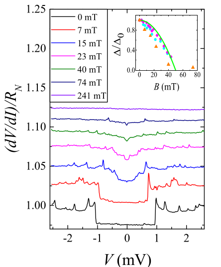
Energy spectrum of topological semi-metals can cause the forming of surface flat-bands. This subject draws much attention, since it is predicted, for instance, that the flat-band forming should cause a temperature jump of the superconducting transition due to high state density in the flat-band.
We experimentally investigate charge transport through the interface between a Cd3As2 topological Dirac semimetal and a normal Au lead.
For such interface, the obtained differential resistance spectra dV/dI(V) show Andreev-like reflection with a well-defined superconducting gap. This is highly unexpected in a system of two non-superconducting bulk materials. We connect this behavior with surface (interface) superconductivity. Surface superconductivity proved to be resistant to the Cd3As2 surface quality due to the flat-band formation in Cd3As2, which has been predicted theoretically for topological metals.
The conclusion on superconductivity is also supported by the temperature and magnetic field-effect curve dependences dV/dI(V). The flat-band formation on the Cd3As2 surface is also proven by ARPES results.
Related article:
O.O. Shvetsov, V. D. Esin, A. V. Timonina, N. N. Kolesnikov, and E. V.
Deviatov. Surface superconductivity in a
three-dimensional Cd3As2 semimetal at the interface with a
gold contact. Phys. Rev. B 99, 125305 – Published 29 March 2019.
DOI: 10.1103/PhysRevB.99.125305
Section
II “Physical Sciences”, Subsection 8, Theme 0032-2019-0015
“Collective phenomena in electron and exitone systems in
semiconductor nano-strustures”
Prediction and observation of the first antiferromagnetic topological insulator
V.N. Zverev et al.
Basing on the density functional theory, we predict and confirm by investigation of the structure, transport, magnetotransport and magnetic properties, and by using photoemission spectroscopy with angular and spin resolution the realization of an antiferromagnetic phase of a topological insulator in the layered MnBi2Te4 crystal.
We found that the MnBi2Te4 crystal surface exhibits a large bandgap in the topological surface state. The same fact is confirmed by ab-initio calculations and photoemission measuring.
We expect the observation of a number of exotic fundamental phenomena, among them quantized magnetoelectric coupling and axion electrodynamics, quantum anomalous Hall effect and chiral Majorana fermions.
Related article:
M. M. Otrokov, I. I. Klimovskikh, H. Bentmann, A. Zeugner, Z. S. Aliev, S. Gass, A. U. B. Wolter, A. V. Koroleva, D. Estyunin, A. M. Shikin, M. Blanco-Rey, M. Homann, A.Yu. Vyazovskaya, S. V. Eremeev, Yu. M. Koroteev, I. R. Amiraslanov, M. B. Babanly, N. T. Mamedov, N. A. Abdullayev, V. N. Zverev, B. Buchner, E. F. Schwier, S. Kumar, A. Kimura, L. Petaccia, G. Di Santo, R. C. Vidal, S. Schatz, K. Kiner, C. H. Min, Simon K. Moser, T. R. F. Peixoto, F. Reinert, A. Ernst, P. M. Echenique, A. Isaeva, and E. V. Chulkov, “Prediction and observation of the first antiferromagnetic topological insulator”, Nature, 576, 19/26, 416-437 (2019).
Section
II “Physical Sciences”, Subsection 8, Theme 0032-2019-0015
“Collective phenomena in electron and exitone systems in
semiconductor nano-strustures”
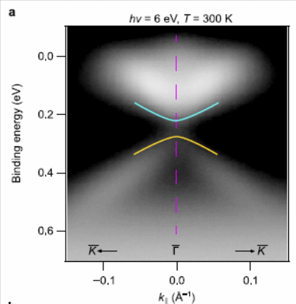
Exchange energy renormalization in quantum Hall ferromagnets with abnormally strong interaction
А.B.Van’kov, B.D.Kaysin, I.V.Kukushkin et al.
An unusual behavior of exchange energy scale, and a shift in dependences of exchange energy from electron density is discovered in a two-dimension ferromagnet electron system with abnormally strong interaction at the filling factor
It is found that such exchange energy is close to cyclotron energy in a broad scale of electron concentrations (at rs> 7). This is notably different from the typical concentration dependence and the scale according to the formula that is typical for relatively weakly interacting systems.
The exchange energy was probed by means of inelastic light scattering from collective spin flip exitation energy in MgZnO/ZnO heterostructures.
It is found that the discovered exchange interaction renormalization is connected to the electron state blending on high unoccupied Landau levels.
The same trend was confirmed via numerical calculations with adequate account of Coulomb interaction shading effect.
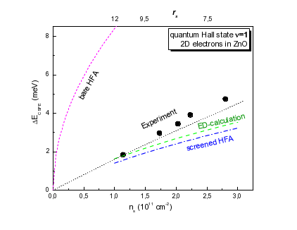
The green dashed line (ED) indicates calculations by precision diagonalization method. The blue dash-dot line (HFA) marks calculations by Hartree–Fock approximation with regard to interaction screening. The purple dotted line indicates the calculated energy without regard to Landau level blending.
Related article:
А.B.Van’kov, B.D.Kaysin, S.Volosheniuk, I.V.Kukushkin. “Exchange energy renormalization in quantum Hall ferromagnets with strong Coulomb interaction”, Phys.Rev. B 100, 041407 (2019).
Section II “Physical Sciences”, Subsection 9, Theme 0028-2019-0020
“New functional materials and structures”
In situ analysis of chemical transformationss in solid oxide fuel cell (SOFC)electrodes by Raman spectroscopy
D.A. Agarkov, S.I. Bredikhin, I.N. Burmistrov, G.M. Eliseeva, I.I. Tartakovsky, V.V. Kharton
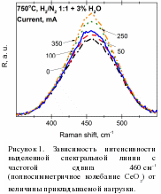
Charge transport and current-generating redox reactions in solid oxide fuel cell (SOFC) composite anodes were studied in dependence to the current density and fuel gas mixture composition in the anode chamber.
It is found that the current in the SOFC changes the charge state of Ce cations in the anode (see Fig. 1). It proves direct oxygen transfer from the solid electrolyte to composite anode via “oxygen spillover” mechanism.
Local ratio of cerous cerium and ceric cerium, as well as local chemical potential of oxigen on the electrode-electrolyte interface is estimated in dependence to partial pressure of hydrogen in the anode chamber and current density in the SOFC.
Related articles:
D.A. Agarkov, M.A. Borik, S.I. Bredikhin, I.N. Burmistrov, G.M. Eliseeva, V.A. Kolotygin, A.V. Kulebyakin, I.E. Kuritsyna, E.E. Lomonova, F.O. Milovich, V.A. Myzina, P.A. Ryabochkina, N.Yu. Tabachkova, T.V. Volkova “Structure and Transport Properties of Zirconia Crystals Codoped by Scandia, Ceria and Yttria”
Journal of Materiomics, vol. 5, pp. 273-279 2019 (Q1).D.A. Agarkov, I.N. Burmistrov, G.M. Eliseeva, I.V. Ionov, S.V. Rabotkin, V.A. Semenov, A.A. Solovyev, I.I. Tartakovskii, S.I. Bredikhin “Comparison of In-situ Raman Studies of SOFC with Thick Single-crystal and Thin-film Magnetron Sputtered Membranes”
Solid State Ionics, vol. 344, p. 115091 2020 (Q1).
Section
II “Physical Sciences”, Subsection 8, Theme 0032-2019-0015
“Collective phenomena in electrone and exitone systems in
semiconductor nano-strustures”
Topological Protection Brought to Light by the Time-Reversal Symmetry Breaking
S. U. Piatrusha, E. S. Tikhonov, V. S. Khrapai et al.
We present an experiment that brings to light an enormous magnetoresistance effect in edge conductivity of HgTe/CdHgTe quantum wells with an inverted band structure in the quantized spin Hall effect mode.
Resistance growth within several orders of magnitude in magnetic fields of 10 millitesla scale goes along with transition to exponential time dependence and giant mesoscopic conductance fluctuations.
The observed phenomena are the first to prove the transition to 1D Anderson insulator state, and give good evidence of topological protection of the edge states from scattering in a zero magnetic field.
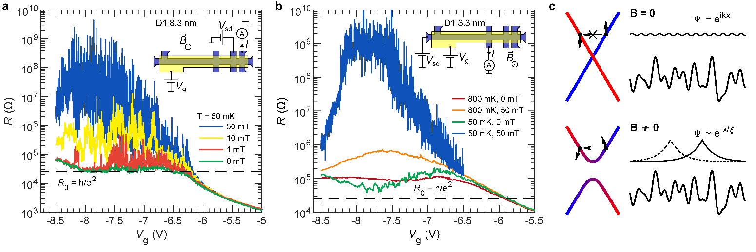
Inserts (a) and (b) show sample structure and the corresponding measuring test circuit. (c) Impact of magnetic field on electrone states in quantum spin Hall effect.
Gapless spectrum is predicted for B = 0 with electron impulse and spin connected (upper left). Random potential does not affect the moving electrons due to topological protection (upper right). In this case the wave function of Ψ electron corresponds with free distribution along the edge, Ψ∼eikx. At B≠0 a Zeeman gap opens in the spectrum. The spectrum legs that are distributed towards it no longer consist of electron states with opposite spins, but hybridize near the Dirac point (lower left). As consequence, topological protection is broken, the disorder causing return to electron scattering and localization (lower right). Wave function envelopes decay exponentially on the localization length ξ, Ψ∼e−x/ξ.
Related article:
Phys. Rev. Lett. 123, 056801 (2019)
DOI: 10.1103/PhysRevLett.123.056801
Section
II “Physical Sciences”, Subsection 8, Theme 0032-2019-0014
“Physics and technology of new materials and structures”
Observing spontaneous vortex and meissner domains in a ferromagnetic superconductor
L.Ya. Vinnikov, M.S. Sidel’nokov, S.V. Egorov, O.V. Skryabina et al.
Spontateous arisal of superconducting meissner domains, and, consequently, abrikosov vortice domains is discovered in a ferromagnetic supercunductor EuFe2(As0.79P0.21)2 monocrystal at superconducting transition temperature of Tsc=22 К and Curie temperature of TC=18 К, during descent of temperature below TC .
This validates the co-existence of two antagonistic cooperative spin phenomena, namely, superconductivity and ferromagnetism, at the atomic scale.
Visualizing the transition of meissner to vortex state of the domains while their own magnetization in the ferromagnetic conductor rises at temperature descent [1] becomes possible due to highly developed high-resolution method of decorating the magnetic current structure at low temperatures [2] which is unique to ISSP.
Related articles:
- L.Ya. Vinnikov, I.S. Veshchunov, M.S. Sidel’nokov, V.S. Stolyarov, S.V. Egorov, O.V. Skryabina, B. Jao, G. Tsao, T. Tamegai. Direct observation of vortex and meissner domains in a ferromagnetic superconductor monocrystal EuFe2(As0.79P0.21)2. JETP Letters 109, pp. 530-534 (2019).
- L.Ya. Vinnikov, I.S. Veshchunov, M.S. Sidel’nokov, V.S. Stolyarov, High-resolution technique of magnetic current structure decoration at low temperatures. Experimental devices and techniques 4, с. 141-147 (2019) (in Russian)
Key implementable findings in 2019
Section II “Physical Sciences”, Subsection 8
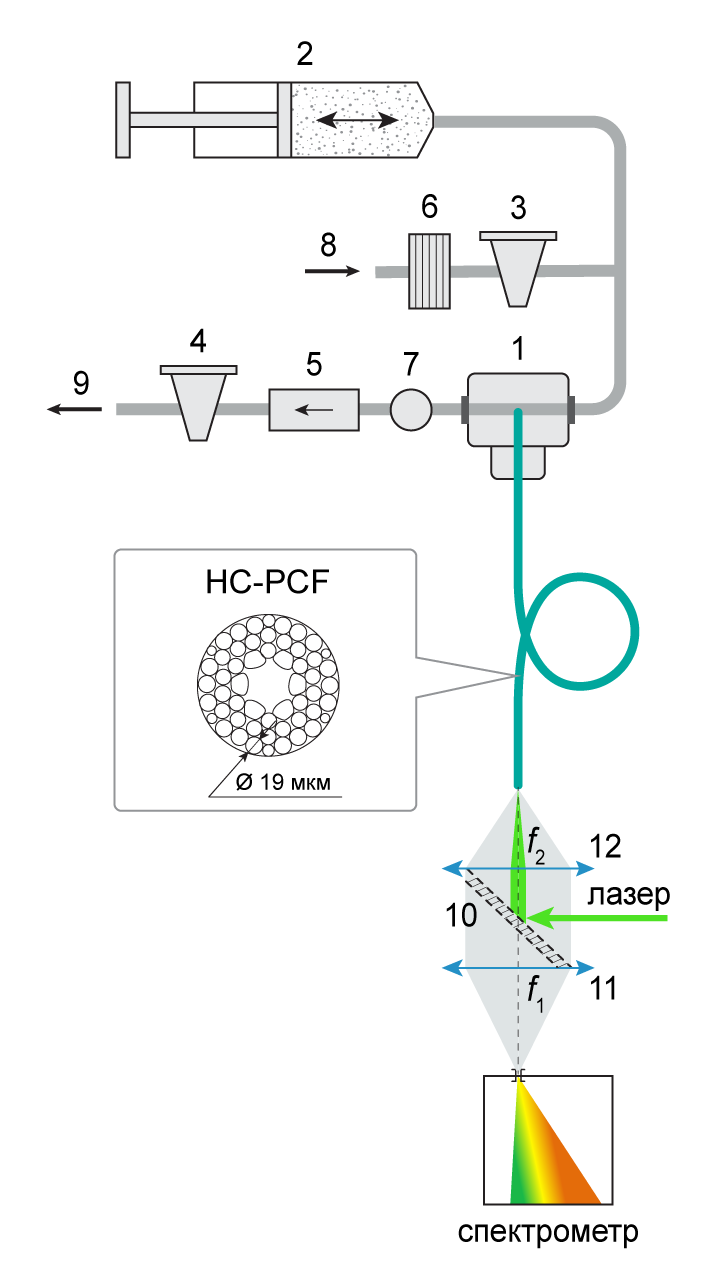
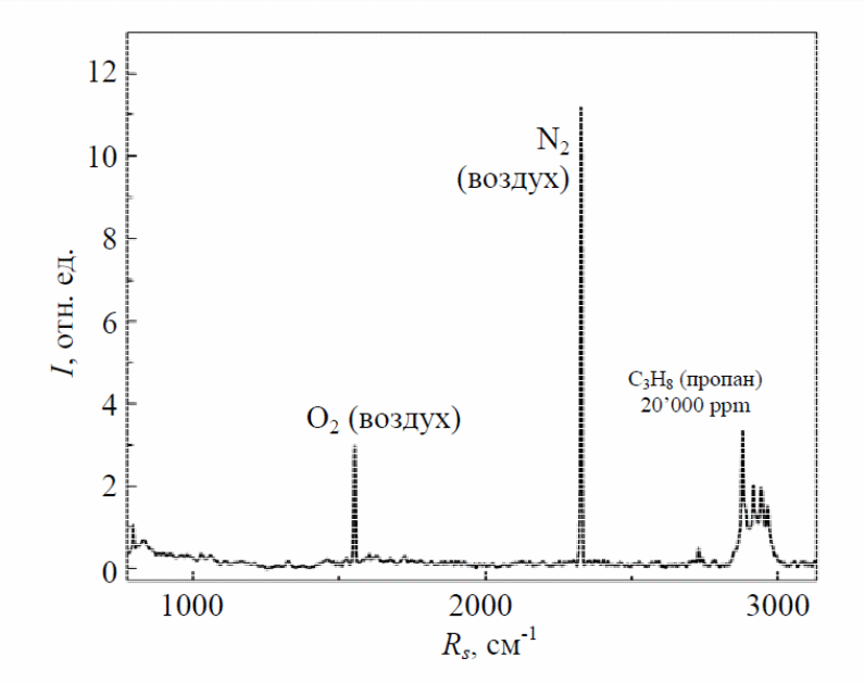
Portable universal gas tester based on Raman scattering and hollow photonic-crystalline fibers
A.B. Van’kov, S.I. Gubarev, V.E. Kirpichev, E.N. Morozova, M.N. Hannanov, L.V. Kulik, I.V. Kukushkin
A construction of portable device based on Raman spectrometer and hollow photonic-crystalline optic fiber is designed and constructed that makes the inelastic light scattering signal level two orders of magnitude higher on various gas mixtures compared to open gas volume signal.
Currently, the quantitative accuracy level for gas mixtures is 0.5%, and the sensitivity level is ~300ppm (part per million) for any organic or non-organic polyatomic gases, including gases like hydrogen, chlorine gas and gaseous fluorine, that are IR-inactive.
Various ways of increasing the system sensitivity are suggested, so that it can be used for online-monitoring of gas mixture compositions with component concentrations up to 100ppb.
This system can be implemented as means of atmospheric air ecological monitoring, in security service, in medical analysis. It is non-selective, has high rate accuracy comparable to chromatography, and needs no expendables, which makes its implementation economically feasible.
Related article:
A.B. Van’kov, S.I. Gubarev, V.E. Kirpichev, E.N. Morozova, M.N. Hannanov, L.V. Kulik, I.V. Kukushkin. “Portable gas tester based on fiber Raman spectrometer”, Journal of Applied Physics, 2019, #4, PP. 87-91 (in Russian).
A patent application is made for “Portable universal gas tester based on fiber-intensified Raman scattering for multi-component mixtures”.
Section II “Physical Sciences”, Subsection 9
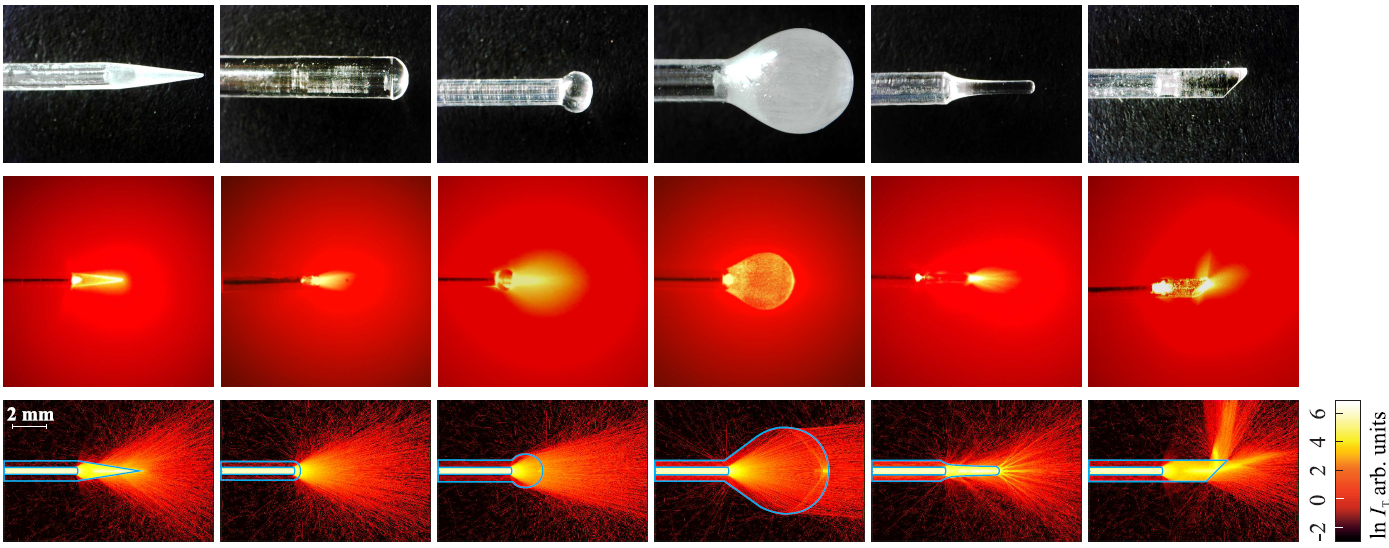
Sapphire capillary needles for interstitial laser treatment and surgery of cancer tumors
I.A. Dolganova, I.A. Shikunova, G.M. Katyba, A.K. Zotov, V.N. Kurlov et al.
Local laser irradiator for therapy and surgery of cancer tumors via interstitial thermo- and photodynamic therapy is designed.
The irradiator consisits of a radiolucent sapphire capillary with a closed end, and within it a Q fiber conneceted to laser radiation source or to a spectrometer.
Growing sapphire capillaries by the designed method makes crystals with a surface that does not need firther polishing. It allows precise forming of a closed end capillaries.
A set of irradiators for obtaining radiance beams with a required diagram includes a diffuser-fitted irradiator.
The irradiators provide better control of radiation scattering and the generated heat in the tissues. Their radiation power capacity range is significantly broader compared to similar devices. They can fulfill multiple tasks in surgery and oncology.
Related article:
I.A. Dolganova, I.A. Shikunova, G.M. Katyba, A.K. Zotov, E.E. Mukhina,
M.A. Shchedrina, V.V. Tuchin, K.I. Zaytsev, V.N. Kurlov
“Optimization of sapphire capillary needles for interstitial and
percutaneous laser medicine” - J. of Biomedical Optics, 24(12),
128001 (2019).
DOI: 10.1117/1.JBO.24.12.128001
Section II “Physical Sciences”, Subsection 9
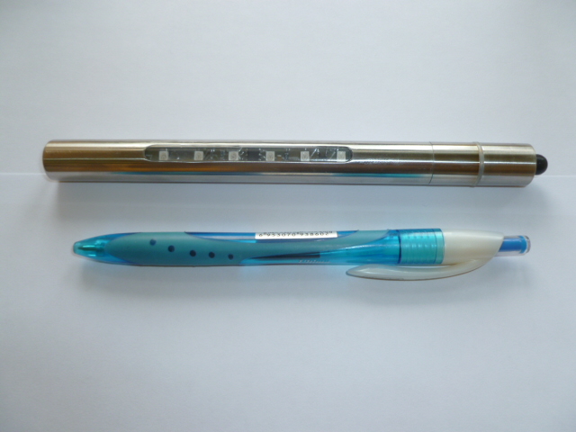
Advanced gamma-radar for rapid localization of malignant lumps during surgery
A.D. Orlov, N.V. Klassen, S.Z. Shmurak, V.V. Kedrov, E.D. Shu, K.A. Chuvalova
Precise gamma-radar for rapid localization of malignant lumps during surgery is designed.
It has advantages compared to previously designed models. Its gamma-radars use reinforced scintillant crystals based on lanthanum bromide set up at ISSP. It is both highly sensitive and reliable. It has a heavy-metal collimator for both precise localization and protection, which reduces the size and weight of the device. It has multistage light and sound signalization that allows the surgeon to rapidly and precisely locate the malignant cells without taking their eyes off the scalpel.
Prontotype gamma-radar samples were used in leading oncological clinics and got positive feedback as being precise and convenient.
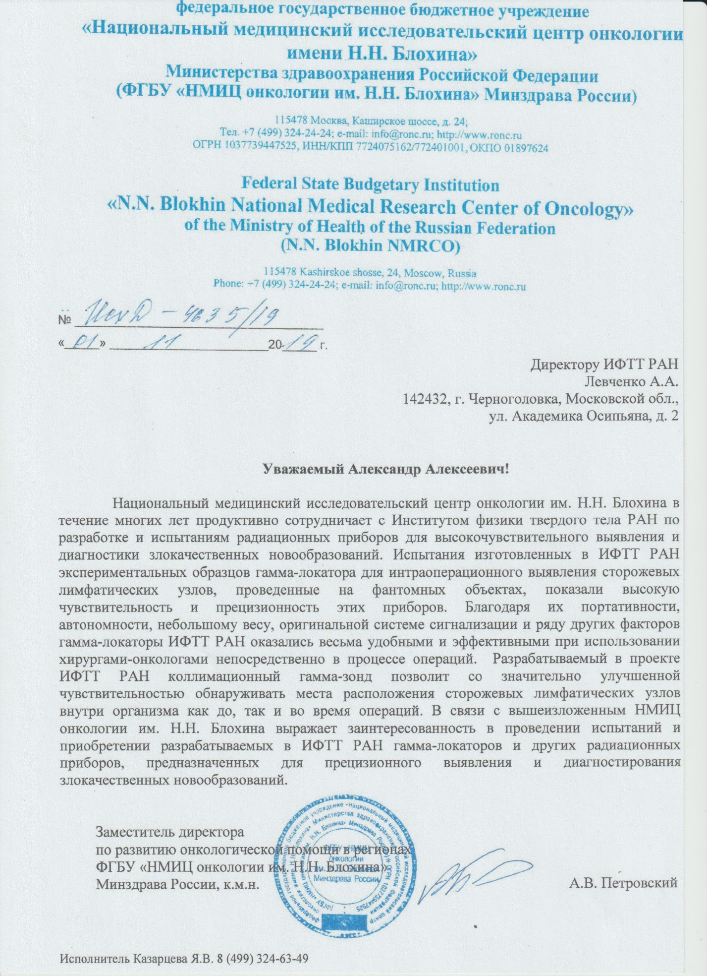
The device was also mentioned in the official letter of A.V. Petrovsky, Vice-principal of N.N. Blokhin National Medical Research Cetner of Oncology as having high innovation potential. The Center is developing oncological therapy in regional Russia. The Vice-principal’s feedback estimates the device being ready for broad implementation. A copy of the letter is attached below.
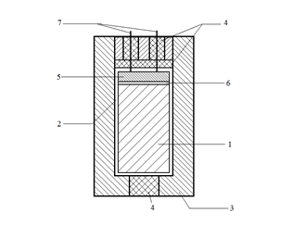
1 – scintillant crystal; 2 – light-reflecting coating; 3 – heavy-metal leak-proof container/gamma-radiation collimator; 4 – sealing glue; 5 – solid-state photoelectron multiplier; 6 – optically-transparent< glue; 7 – sealed electrical contacts;