
")
")


MAIN ACHIEVEMENTS 2013
|
On a New Type of Dirac Fermions in Crystalline Topological Insulators Algebraic topological methods are fruitfully applied to many problems from quantum field theory to condensed matter physics. Although the foundations of mathematical methods are common, the methods themselves can vary depending on the formulations of problems. We briefly mention frequently used approaches. For example, the problem of the classification of structural defects and determination of their stability is reduced to the analysis of the equivalence classes of homotopic maps of a certain standard manifold associated with the bypass of a defect to the space of the order parameter. The classification is reduced to the list of homotopy groups associated with such maps. The formulation of the problem for crystal insulators differs from those mentioned above and is mainly reduced to the following questions. (i) What nontrivial features of the electron spectrum dictated by spatial symmetries and time reversal invariance are possible on the surface in these systems at the symmetric k points of the Brillouin zone(ZB)? They should not be present in the systematic of the bulk spectrum (should be beyond the projections of bulk bands, see below). (ii) Are these singularities stable under continuous deformations of the Hamiltonian of the system under which the Hamiltonian is invariant under spatial symmetry elements and time reversal, and which do not close the gap in the projections of bulk bands? This leads to the so-called Z2 classification different from the mentioned classification of torsions in the momentum space.
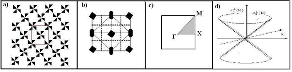
Fig.1. a) An example of two-dimensional lattice with nontrivial translations. b) Elements of lattice symmetry (the sliding planes are marked by dashed lines). c) Irreducible part of the Brillouin zone. d) A conical spectrum of the fourfold expressed fermions. Until now, for crystalline 3D→2D, 2D→1D, and pure two-dimensional 2D systems, the features of the spectrum with two-fold degeneracy at the symmetrical points of the ZB (conical, ε ~ ±|k|; square, ε ~ ±|k|2; and cubic ε ~ ±|k|3) have been discussed. Conical features of the spectrum were detected experimentally in pure 2D systems (graphene), as well as in 3D→2D systems (BiSb binary compounds, and heteroboundaries between A4B6 and A2B6 semiconductors with band inversion), and 2D→1D crystal systems. A question arises of whether conical features exist in crystalline systems with a higher degree of degeneracy. The study of the possibility of the appearance and experimental detection of such features (if they are possible) in crystalline 3D→2D, and pure 2D systems is an interesting topical problem. Surface (edge) states with the conic dispersion law, and with more than two-fold degeneracy are absent in 2D→1D systems, because the groups of borders do not allow more than two-fold degeneracy because of the poverty of symmetry elements. The ideal situation would be if particular materials, or compounds where a larger degree of degeneracy was possible could be presented. However, it is currently impossible. Nevertheless, it is possible to present a crystal structure of a compound with a conical massless spectrum with fourfold degeneracy. This problem is solved in this work. Moreover, four-fold degeneracy of the conical spectrum turns out to be maximally allowable in 3D→2D systems. (Laboratory of Semiconductor Surfaces Spectroscopy, Doctor Sci. of Physics and Mathematics, Prof. S. N. Molotkov) |
|||||||||||||||||||
|
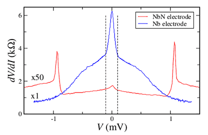
Suppression of Andreev reflection at energy levels much lower than the super-conducting energy gap Recently, there is a strong interest in semiconductor hybrid systems which consist of a metal and a low-dimensional electron system. Such interest was originally caused by the problem of finding elementary excitations of a Majorana fermion type in a solid body. Yet it turned out that the topological superconductivity mode that allowed such excitation caused special interest, both theoretically and experimentally. The topological superconductivity mode emerges when the macroscopic order parameter penetrates the interface between a low-dimensional electron system with a strong spin-orbit coupling, and a superconductor. So far, experimental results in this field have been controversial. They mainly refer to the case of one-dimensional systems, i.e. a quantum wire. On the other hand, it is well-known that the edge of a two-dimensional electron system exhibits well-pronounced qualities of a one-dimensional transport both in quantizing and zero magnetic fields. Therefore, a more general experimental task of investigating the transport through the interface between a two-dimensional electron system with a strong spin-orbital coupling, and a metal with a macroscopic order parameter can be set. The charge transport through the interface between an edge of a two-dimensional electron system in a narrow quantum well InGaAs that exhibited a strong Rashba type spin-orbit coupling, and a metal with a macroscopic order parameter – a superconductor (Nb, or NbN) was investigated.
A partial suppression of Andreev reflection on the interface at super-cold temperatures (less than 300 mK), and small electrical bias was revealed. Analyzing the magneto-field and temperature dependencies provides a definitive interpretation of this suppression being the result of spin-orbit coupling in a two-dimensional system. Also, a local interface conductivity peak at zero biases, located in a narrow area of magnetic fields that corresponded to the ones necessary for topological superconductivity realization (zero bias anomaly) was revealed. These results were partly (in the part of the first measures of the niobium contact) published in a work “Letters to Journal of Experimental and Theoretical Physics”, №98, Issue 7, 477-483 (2013). (Laboratory of Quantum Transport, Doctor Sci. of Physics and Mathematics A. A. Shashkin)
|
|||||||||||||||||||
|
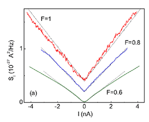
Finite size effect in the shot noise in hopping conductivity Under the condition of thermodynamic equilibrium, current fluctuations in a conductor are determined solely by its temperature and resistance (the Johnson-Nyquist thermal noise). In presence of an electric current non-equilibrium excess fluctuations occur, so-called shot noise. Such noise results from the discreteness of the elementary charge, and is maximum for Poisson statistics of the charge flow. The conductance of a metallic and/or coherent conductors at low temperatures is determined by the elastic scattering processes. In such systems the shot noise is observed provided the size of the sample investigated is small compared with the energy relaxation length on which a local equilibrium is established. Whether the shot noise exists in an insulator with a hopping conductivity at a finite temperature, and what's its magnitude is not obvious. In fact, the hopping conductivity itself is an inelastic process already on the scale of a single hop (~ 100 nm), that, presumably, should suppress the noise in macroscopic samples. In this work the shot noise in a two-dimensional electronic system in GaAs in samples with a channel length of 5 um at temperatures in the range from 0.5 to 4.2K is investigated. Electronic density changes by means of a metallic front gate. At a low densities, an insulating state is achieved with the conductance temperature dependence corresponding to the Mott's variable range hopping regime. In such conditions the spectral density of the current noise is measured at frequencies above 10 MHz, which is about two orders of magnitude higher than all of the previous studies, allowing to reliably avoid the influence of the modulation/flicker noise. At a temperature of 0.5K the conductivity falls roughly exponentially at decreasing the electron density, while the shot noise increases and reaches the Poisson value (Fano factor comparable to 1 for resistivity in the range of 10 MOhm per square). To our best knowledge, this is the first demonstration of a full shot noise in an insulator of a macroscopic size. It is also demonstrated for the first time that the shot noise significantly decreases when the temperature is increased (approximately a factor of 3 within the temperature range studied).
These results can be qualitatively explained by taking into account the features of the electric current flow in the VRH regime. It is well-known that the infinite current-carrying cluster is formed on the Miller-Abrahams random network with an exponentially wide spread of the hopping resistances. The correlation length LC of such a cluster by far exceeds the average hop length, and determines the typical scale of the conductivity self-averaging. In samples of the size smaller than LC the electric current flows along quasi-one-dimensional chains, with one highest hopping resistance dominating the resistance of each chain. As a result, the full current noise of a macroscopic sample is determined by such single hops, and reaches the Poisson value. Based on experimental estimates of the localization length and Mott's temperature, the Poisson noise sets in at LC ~ 1.5mkm, which is comparable to the sample size. The fact that LC decreases as the temperature and/or localization length increase explains qualitatively the observed decrease of the shot noise. At the same time, the shot noise decreases slower than the correlation length, which might be a result of poor self-averaging. (Laboratory of Quantum Transport, Cand. Sci. of Physics and Mathematics V. S. Khrapai)
|
|||||||||||||||||||
|
Nonlocal Supercurrent Observation in a Mesoscopic Structure with Josephson Junction 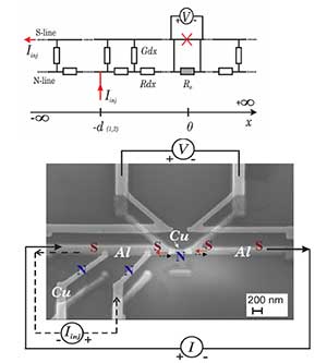
The nanoelectronic superconductive devices that are being developed nowadays, are often under nonequilibriun conditions, since their size is comparable to such specific lengths as the length of nonequilibrium normal carrier conversion into cooper pairs lQ, spin diffusion length lS, et cetera. The effect discussed is due to the submicron Josephson planar junction (the SNS bridge located in the middle of the Figure) is fabricated near an normal carrier (quasi-particle) injector, so that the space d between the injector (N), and SNS junction was obviously smaller than lQ, but significantly larger the superconducting coherence length xs. When injecting the quasi-particles into the nearest superconducting aluminum bank of the SNS junction ‘bypassing’ the junction itself (the “nonlocal” current pass) is marked by a dotted line in the Figure), voltage over the junction was revealed when the electric current of the injection exceeded the critical value of Iinj,c. The value of Iinj,c was significantly higher than the normal critical current Ic that was measured at the “local” current flow through the SNS junction (shown by a solid line in the Figure). The upper part of the Figure shows an equivalent two-channel circuit that describes the occuring non-equilibrium processes, and corresponds to the theoretical model. The upper horizontal line represents the superconductive component. Its electrochemical potential only changes in the Josephson junction marked by the cross in the Figure. On the contrary, electrochemical potential of the normal component (lower curve) changes along the whole structure. The presence of a non-equilibrium potential difference between the lines leads to conversion of the quasi-particles into Cooper pairs. This conversion is determined by an effective “cross conduction” G=(RlQ2)-1, where R is the normal resistance per unit length of the aluminium strip. Investigation within the framework of the suggested model shows that Ic/Iinj,c ratio corresponds to the fraction of the injected quasi-particles that reach the SNS junction, and get compensated by counterflowing superconductive component, since the total current through the junction in the “non-local” experiment equals to zero. The discovered effect may be helpful for adjusting critical parameters in Josephson junctions by unbalanced currents in Josephson electronic diagrams. (Laboratory of Superconductivity, Doctor Sci. of Physics and Mathematics V. V. Ryazanov)
|
|||||||||||||||||||
|
Blowup dynamics of coherently driven polariton condensate It was theoretically predicted basing on Gross-Pitaevskii equation that elastic parametric scattering can lead to energy accumulation of the polariton condensate under resonant and coherent optical pumping. The state of the condensate evolves in a peaking mode; slow intensity growth emerges at the point of the scattering threshold and gives way to burst-like explosive growth and transition to the upper stability branch in a finite amount of time. During the process, the pumping amplitude weakly affected the finite amplitude of the cavity response, but it determined “the peaking period” that passed between the “switching on” of the pumping of the given amplitude and the rapid field enhancement. This period varied in quite a wide range from several polariton lifetimes (under intensive pumping) to macroscopic amounts (near the scattering threshold). Figure. “Time-suspended” effect of the transition between the stability branches of the bistable polariton condensate. The microcavity is excited along the cavity normal at 0.5 meV above the polariton level at resonance width of 0.04 MeV; a polariton lifetime makes 16 picoseconds. The pumping intensity exceeds the scattering threshold on 10%, but is 3 times lower that the transition threshold between the stability branches in a single-mode system (without scattering). The upper part of the Figure illustrates the cavity field intensity vs time and planar projection of the wavevector (k = 0 corresponds to the excited mode); the lower left part shows the pumping intensity (dotted line) and the excited mode (solid line). The right part shows the resulting intensity of the scattered states vs time. Obviously, the slow energy accumulation of the scattered modes that occurred within 600 picoseconds under a strictly constant fixed outer pumping, ultimately lead to catastrophic field enhancement in the photoexcited mode itself. The final response intensity is only 10% lower than the intensity that could have been obtained without time delay under a pumping intensity three times higher. The here described effect mediates the mechanisms of non-equilibrium transitions, particularly the rapid spin conversion of polariton systems [1-3] in resonant-optical excitement. It is to be taken into consideration when developing optical switches and logical elements based on microcavities with a strong exiton-photon coupling. 1. S. S Gavrilov, A. V. Sekretenko et al., Applied Physics Letters 102, 011104, 2013.
|
|||||||||||||||||||
|
Influence of Spin-Orbit Coupling on Electron Localization Effects
We analyzed how this effect is influenced by quantum corrections coming from the electron-electron coupling. The analysis indicated that there exists a parameter domain where the triplet contribution to the quantum correction to the conductivity of a two-dimensional electron system with a spin-orbital coupling is not suppressed by the electron-electron coupling. Figure. Comparison of experimentally measured conductivity temperature dependences (symbols) with the calculated values: the dotted curves are the results calculated according to the weak- localization theory, and the solid curves are the calculation results with quantum corrections related to the electron-electron interaction in diffusion and ballistic modes taken into account (G. Zala, B.N. Narozhny, and I.L. Aleiner, Phys. Rev. B 64, 214204 (2001)), and without suppression of the triplet channel contribution by the diffusion mode electron-electron coupling. In all calculations, we used the times of the electron wave phase relaxation and spin-orbit relaxation, evaluated by measuring the nonmonotone anomalous magnetoresistance. (Nanolithography Sector, Doctor of Physical and Mathematical Science S. I. Dorozhkin) |
|||||||||||||||||||
|
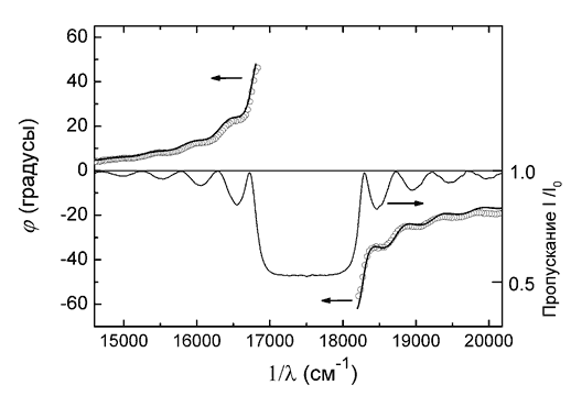
Photonic liquid crystals Epitomes of photonic liquid crystals were prepared. The theoretically predicted but never previously observed singularities linked to pendular oscillations in the diffraction spectra were discovered in the spectra of phase-delay(of the light polarization plane rotation). It was shown that the photonic crystal optical characteristics linked to real and imaginary parts of permittivity could be described basing on universal Kramers-Kroning relations. The Δν photonic band gap widths and their temperature dependence were determined. It was also shown that the temperature dependence of the photonic bandgap Δν/ν0 relative width could be described using Landau theory of the first-order phase transition.
Figure. Spectra of transmittance and phase-delay (of the light polarization plane rotation) of a cholesteric photonic crystal. The calculated and experimental spectra φ are marked by symbols and a solid curve. (Laboratory of molecular structure spectroscopy, Candidate of Physical and Mathematical Sciences P. V. Dolganov)
|
|||||||||||||||||||
|
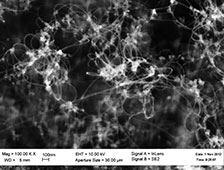
Carbon nanotube arrays on metallic substrates A device for producing carbon nanotube arrays (CNTAs) on metallic substrates (RF Patent for the invention №2471706, 2013) was developed. Technological methods for producing CNT layers on stainless steel, electrotechnical steel and copper substrates were proposed.
The obtained structures are used as field emission cathodes (FEC) in scientific instruments for research in low-temperature physics. Such FECs maintain their performance at temperatures ≤ 4 К. Nothing comparable to these FECs is currently known. (Laboratory of Physical-Chemical Basis of Crystallization, Candidate of Technical Sciences N. N. Kolesnikov)
|
|||||||||||||||||||
|
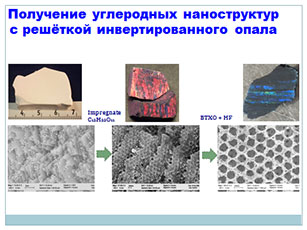
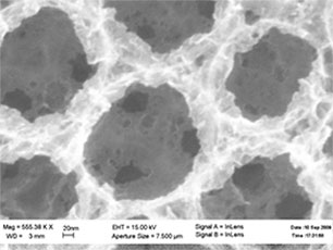
Nanostructured and nanoporous carbon-based materials obtained by globular SiO2 structure invertion. Nanostructured carbon-based materials are attractive from both fundamental and practical points of view. They are widely used in many technologies including electrode materials for supercapacitors, batteries and fuel elements, sorbents of various application and materials for catalysis. The most actively developed prospects are linked to portable power supplies in microelectronics, energy storage systems, components for force pulsing devices and other instruments that require a high-speed energy source. Micropores of at most 2 nm in diameter are the main component of its specific surface area. For quicker ion transport it is crucial to have mesopores (their diameter being from 2 to 50 nm) in the volume of the electrode material. The interconnected micro- and mesopore system combined with high electrode surface area raise the output characteristics of the devices. Micro- and mesoporic carbon-based materials with specific surface area values close to their possible limit (2500 m2/g) and pore volume up to 2 cm3/g got synthesized by the template method in ISSP RAS. An opal matrix represented by a three-dimensional close-packed system of monodispersed globular particles (globules) of silicone dioxide was used as a template. The interconnected micro- and mesoporic system combined with the high surface area of an inverted opal improves both sorption properties and electrochemical output characteristics of the material. Figure 1 shows the synthesis scheme of silicone structures with an inverted opal network, and a fragment of the structure that demonstrates the interconnected pore system.
It was shown that nanostructures have richer variety of properties including new functional properties when compared to the previously investigated materials. For example, spherical carbon particles containing graphite-like (onion-like) shells were discovered in the composite structures. The first investigation results allow an assumption that a diamond-like phase exists in an inverted opal SiC/C composite. Carbon nanostructures with an inverted opal (C-IOP) network modified by tetraphenyl methilene diphosphine dioxide showed high sorption capacity towards Th (IV), U (VI) ions and lanthanides (III) in nitric acid solution, compared to the previously known sorbents. Table 1 shows the distribution ratio of Eu and La/Lu separation factor for our sorbent and other carbon-based sorbents. Table 1
(Laboratory of Crystallization from High-Temperature Solutions (LCHTS) G. A. Emelchenko) |
|||||||||||||||||||
|
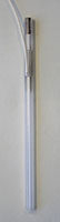
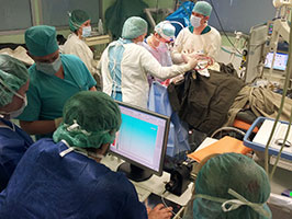
Fundamental principles of laser technologies, including material processing and modification, optical informatics, interconnection, navigation and medicine Sapphire neurosurgical scalpel Multichannel neurosurgical sapphire probe was invented in ISSP RAS. The opened channels of the probe are used for suction, while the closed channels contain optical fibers along which coagulating laser radiation and diagnostic radiation is transmitted to the working tip of the instrument. Fluorophore diagnostics has significant advantages when brain tumor surgery is concerned.
The radiation is transported along the fibers from the laser radiation source to the distal end of the sapphire probe. On leaving the probe it gets internalized into the tissues which leads to their coagulation if the radiation power is high enough. The radiation wavelength is adjusted so that it does not get into the absorption bands of the fluorescent diagnostic agent. It is to prevent its burnout, and also for the penetration depth and zone size of the laser coagulation to be optimal for neurosurgery. The aspirator attached to the sapphire probe removes the brain tissue breakdown product from the diagnosed tumor zone. The main advantage of the above-described device are as follows. 1. Several functions necessary for surgery are combined in one device. 2. The capabilities of the neurosurgical aspirator are enhanced by adding extra spectrometric fluorophore tissue diagnostics, applied interstitially as well. This allows to detect cancer cells appearing in the tissues objectively and timely, and determine how large the lesion site is and what tissue volume has to me removed. 3. It allows to eradicate brain tumors, makes surgical operations less traumatic, reduces blood loss and surgical intervention time by simultaneously demarking and removing the tumor and arresting the bleeding. Sapphire neurosurgical probe and its application to brain tumor removal were developed in cooperation with members of the Neurosurgery Department of Moscow Regional Research and Clinical Institute n.a. M.F. Vladimirsky (MONIKI). RF Patent was obtained for both the method and the device. (Laboratory of Profiled Crystals, Doctor of Technical Sciences V.N. Kurlov) |
|||||||||||||||||||
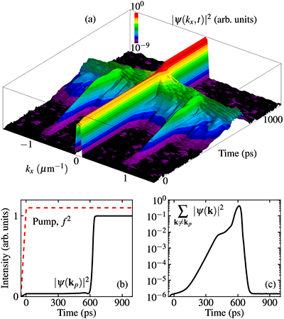 Therefore, a new, significantly nonlinear mechanism of quantum cavity energy accumulation with a strong exiton-photon coupling was discovered. This mechanism reveals itself under photoexcitation with a comparatively large detuning of the pumping frequency from the polariton level.
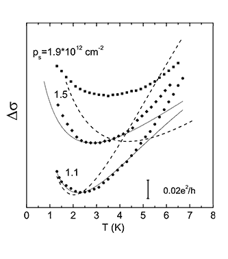 A crossover from weak localization at high temperatures to antilocalization at low temperatures was revealed in the temperature dependence of the two-dimensional hole-channel conductivity in silicon field transistors. We could describe the observed effect quantitatively, taking the change in the ratio of relaxation times of electron wave phases and spins when the temperature changes into account.